Featured Industrial & Optical Quartz Products
Precision-manufactured in Donghai County to ISO9001 and SEMI specifications. Every component is ultrasonically cleaned, verified for optical transmission, and delivered direct to upstate and metro New York facilities.
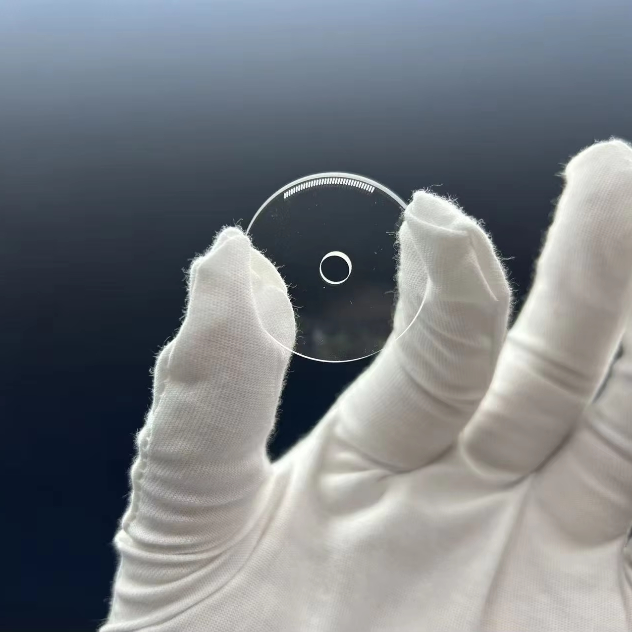
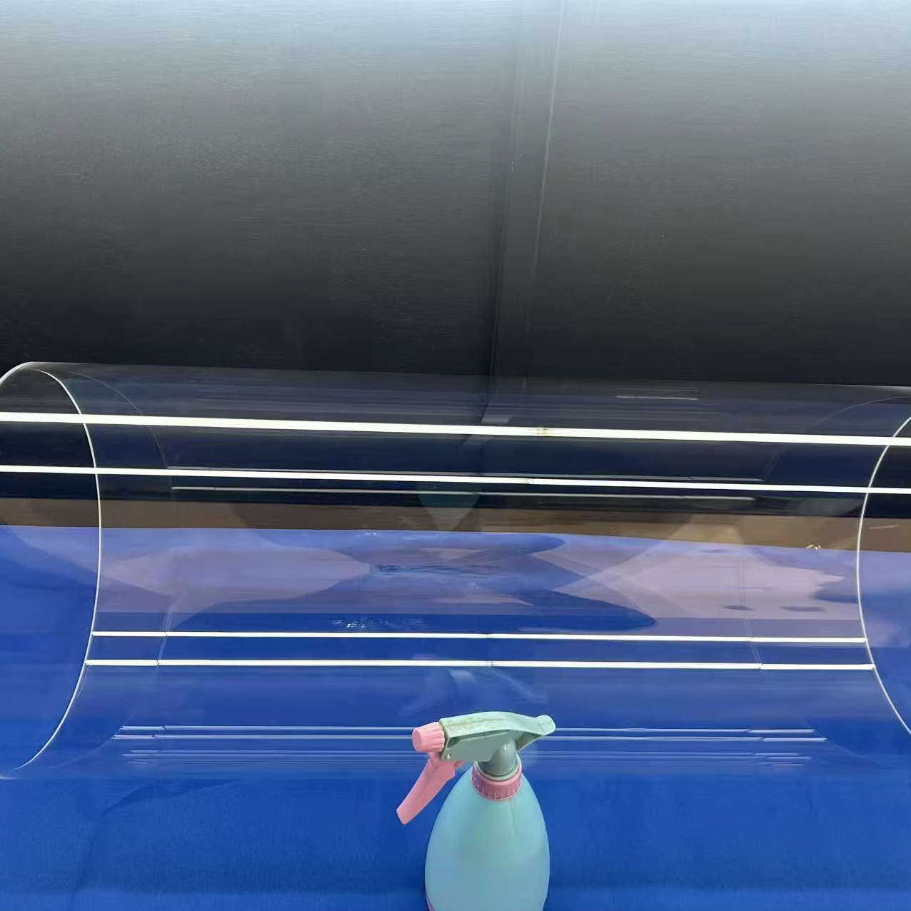
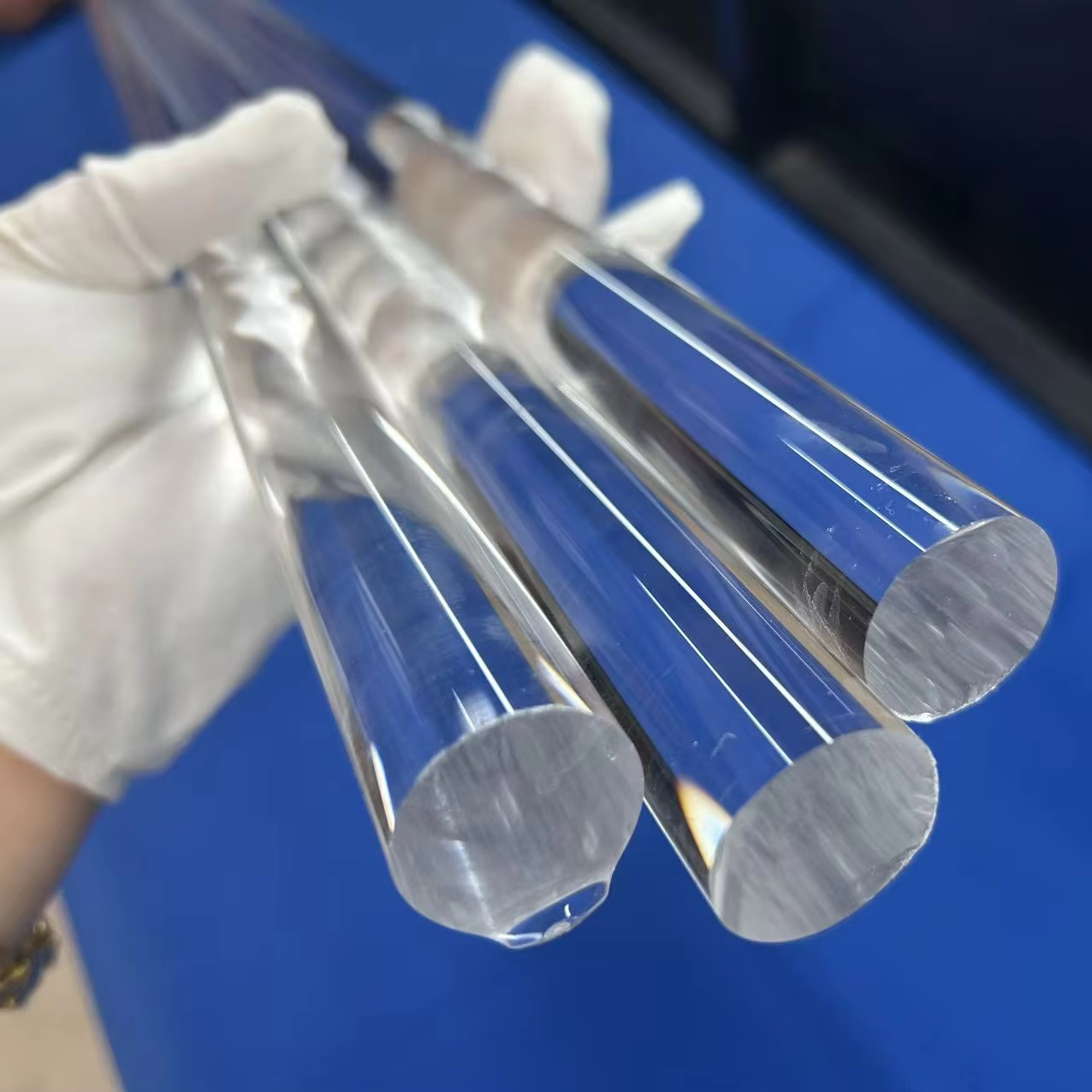
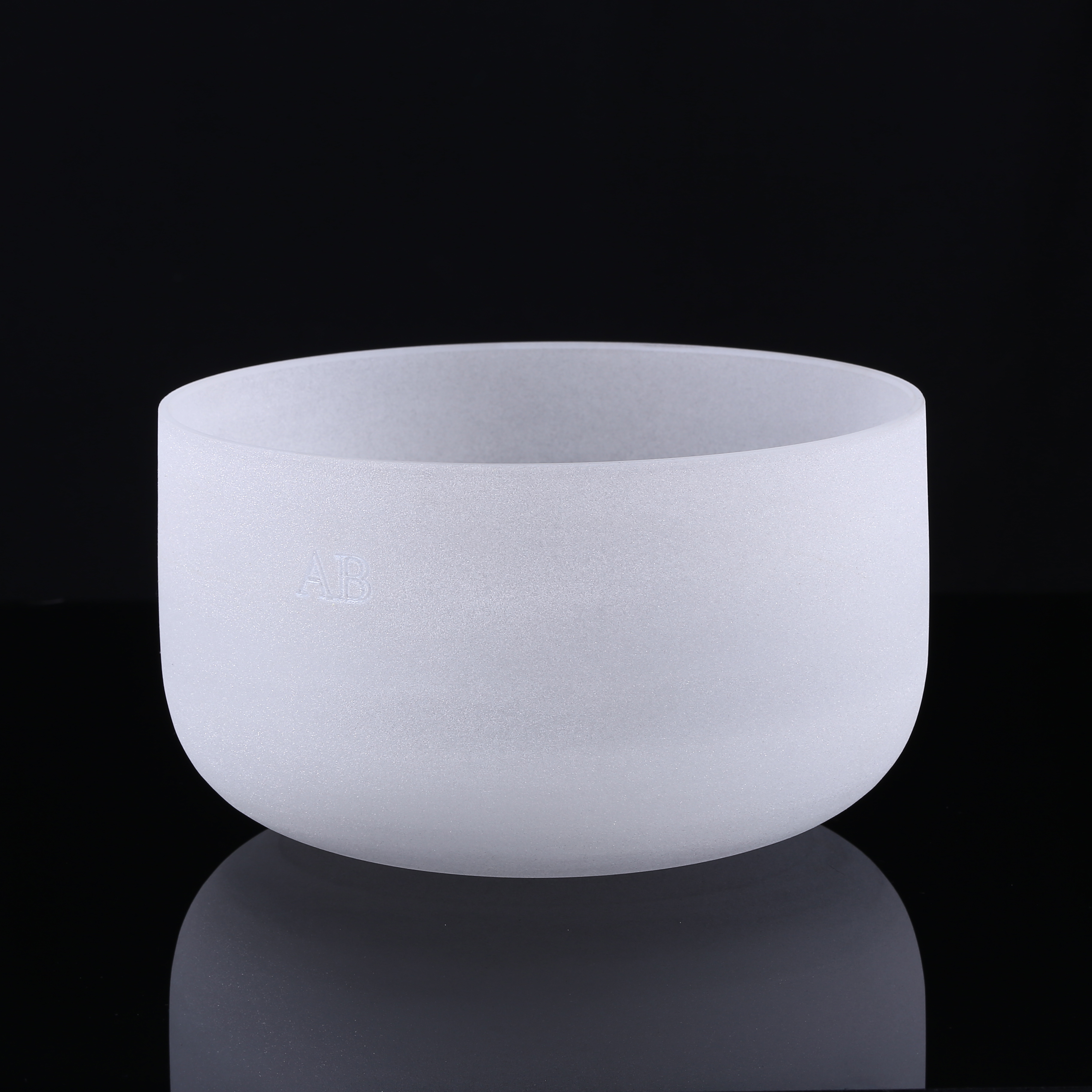
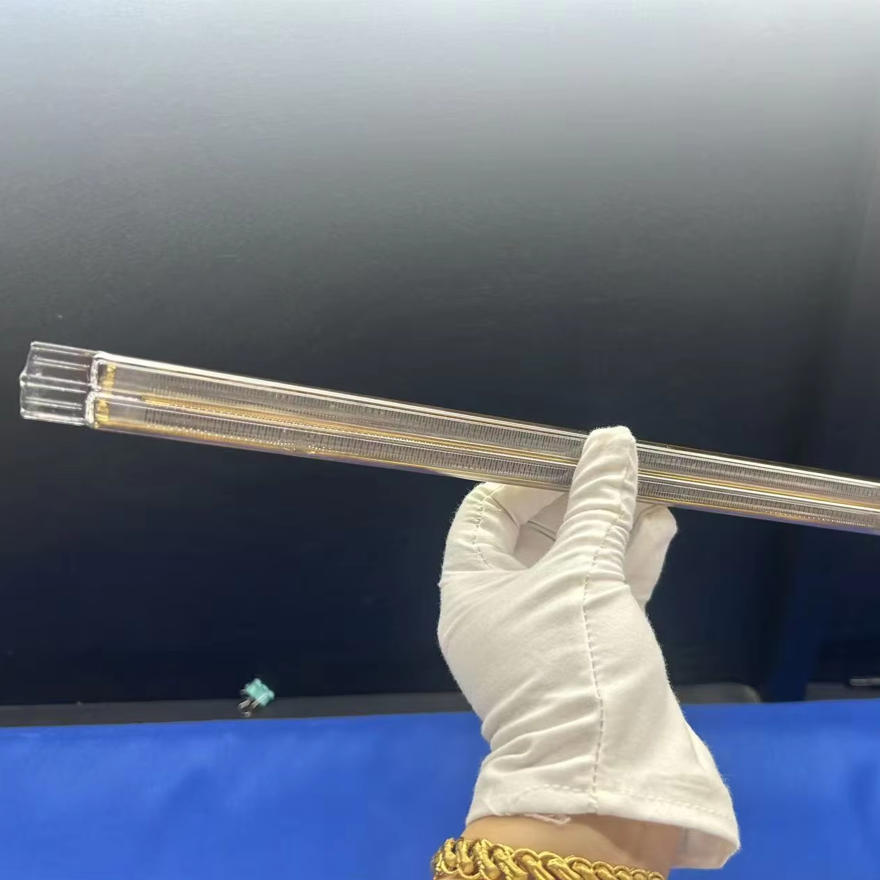
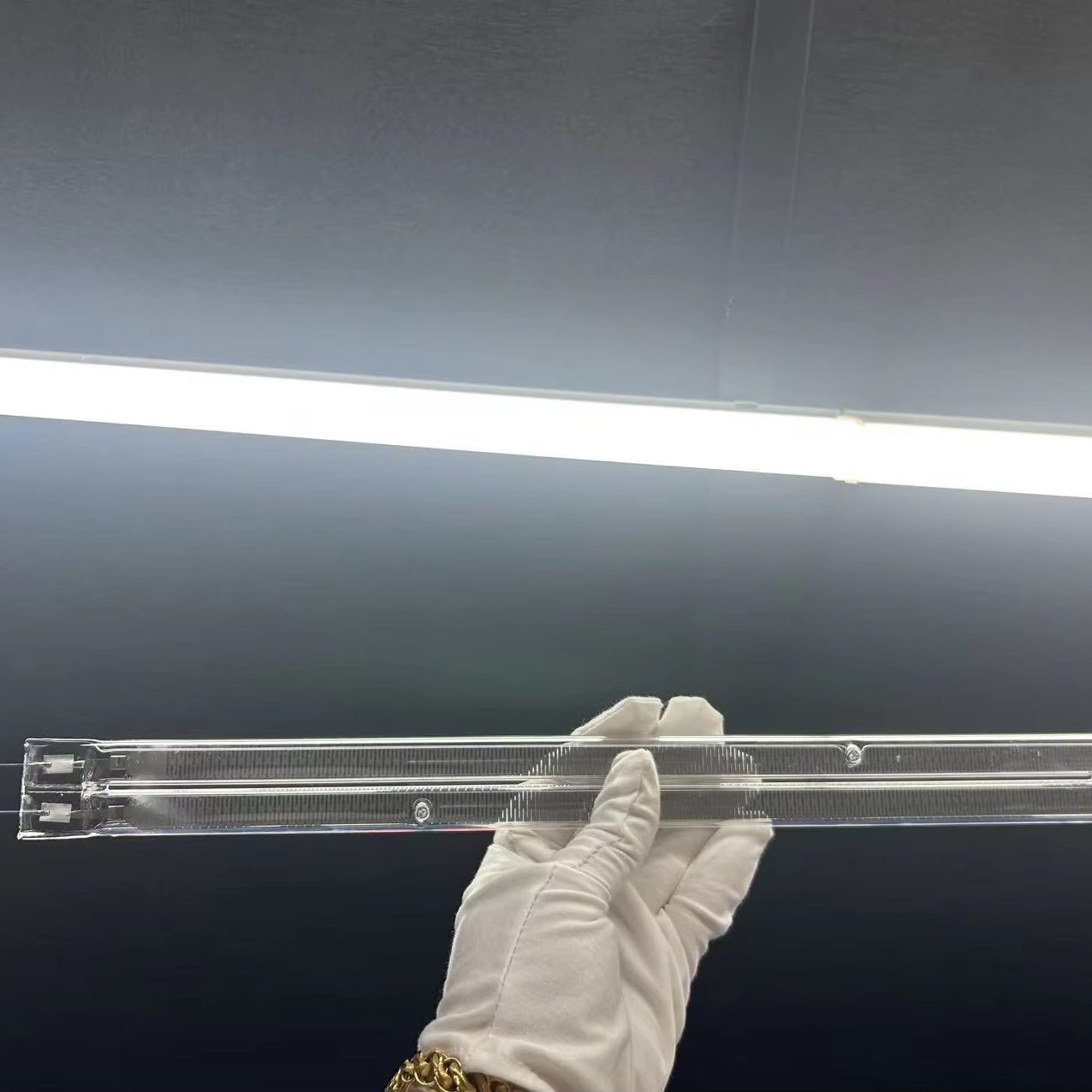
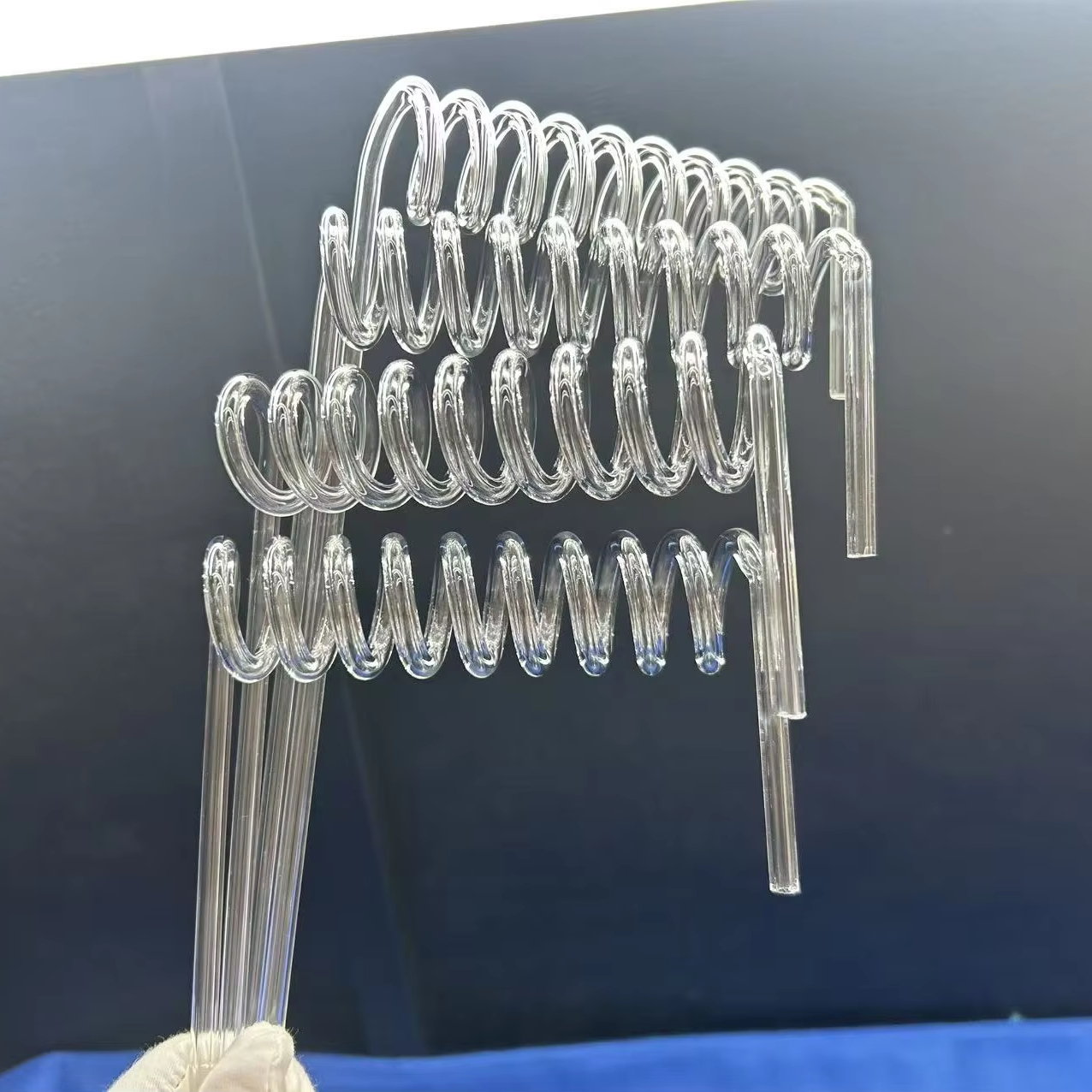
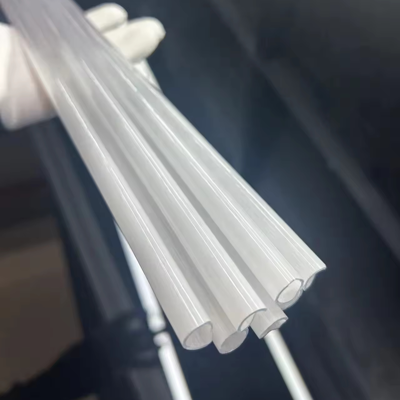
Across New York State, the acceleration of domestic high-tech manufacturing—anchored by the federal CHIPS and Science Act and billions in private capital deployment—has triggered an unprecedented demand for ultra-high purity materials. Fused quartz glass sheets, wafers, and precision-machined silica components represent the bedrock upon which next-generation wafer fabrication, optical communications, quantum computing, and biomedical analytics depend.
From the Albany NanoTech Complex and the Marcy Nanocenter near Utica to the world-renowned photonics cluster in Rochester and the biotechnology institutions across New York City and Long Island, optical and thermal quartz requirements have transitioned from standardized lab consumables to tightly tolerance-controlled, custom-machined substrates. Donghai County Nivra Quartz Products Co., Ltd. serves as a direct manufacturing partner and agile exporter, bridging high-volume raw quartz purification with precision CNC cutting, grinding, chemical mechanical polishing (CMP), and glassblowing to support New York's rigorous production timelines.
New York is spearheading America's microelectronics renaissance. Facilities in Malta (GlobalFoundries Fab 8), Marcy (Wolfspeed), and the planned Micron megafab in Central New York demand immense quantities of low-alkali, ultra-flat quartz carrier plates, wafer boats, furnace process tubes, and wet-bench cleaning tanks. Thermal resilience during extreme chemical vapor deposition (CVD) and diffusion cycles is non-negotiable.
As the birthplace of modern American optical science, the Rochester corridor houses leaders in laser fusion research (Laboratory for Laser Energetics), space-borne imaging optics, and integrated photonics through AIM Photonics. Demands center on synthetic fused silica (JGS1 grade) substrates offering transmission down to 185 nm, minimal wavefront distortion (<λ/10), and exceptional laser damage thresholds (LDT).
From the Manhattan biotech district and Columbia/Cornell Tech incubators to Brookhaven National Laboratory on Long Island, fused quartz plates serve as transparent substrates for microfluidic chips, DNA sequencing flow cells, high-temperature spectroscopy cuvettes, and cryogenic isolation windows in superconducting quantum testbenches.
Engineering Data: Fused Quartz & Silica Selection Matrix
Navigating material performance is crucial for research scientists and manufacturing engineers. Nivra Quartz processes natural crystalline quartz sand and chemical precursors into three distinct grades of fused silica and quartz glass.
| Optical Grade | Raw Material Precursor | Spectral Range | OH Content (ppm) | Primary Industrial Use in NY |
|---|---|---|---|---|
| JGS1 (Synthetic Silica) | SiCl₄ Synthetic Gas Vapor | 185 nm – 2,500 nm (Deep UV) | < 1,200 ppm | Excimer laser optics, semiconductor lithography mask blanks, UV spectrometer windows. |
| JGS2 (Optical Quartz) | Natural High-Purity Rock Crystal | 220 nm – 2,500 nm (UV-Vis) | < 30 – 150 ppm | Sight glasses, viewport windows, furnace viewing ports, high-temp optical sensors. |
| JGS3 (Infrared Grade) | Electrical Fused Vacuum Silica | 260 nm – 3,500 nm (Vis-Far IR) | < 5 ppm (Water-free) | Thermal imaging viewports, IR emitters, military pyrometry, gas chromatography sensors. |
| Opaque / Milky Quartz | Gas-Infused Fused Silica | High Diffuse Reflection | Standard | Semiconductor furnace thermal baffles, flange heat barriers, diffusion tube collars. |
Fused silica’s defining strength is its near-zero coefficient of thermal expansion (CTE ≈ 5.5 × 10⁻⁷ / °C between 20°C and 320°C). Unlike conventional borosilicate or soda-lime glass, a red-hot quartz plate heated to 1100°C can be quenched instantly into freezing ice water without catastrophic thermal fracture.
Strain Point: 1070°C
Annealing Point: 1180°C
Softening Point: 1683°C
Max Continuous: 1100°C
Short Excursion: Up to 1450°C
Density: 2.203 g/cm³
Mohs Hardness: 5.5 – 6.5
Young's Modulus: 72 GPa
Dielectric Constant: 3.75 (at 1 MHz)
Dielectric Loss: < 0.0001
Al: < 14.0 | Fe: < 0.2
Ca: < 0.4 | Mg: < 0.1
Ti: < 1.0 | Na: < 0.3
K: < 0.3 | Li: < 0.2
Total metallic content < 20 ppm
New York Market Trends & Supply Chain Resilience
Strategic supply chain analysis reveals key operational shifts governing how New York procurement teams source, qualify, and integrate quartz components.
Domestic distributors in New York often maintain limited stock of non-standard geometries, incurring lead times of 16–24 weeks for custom quartz plates and tubes. By partnering directly with Nivra Quartz in Donghai, OEM manufacturers reduce lead times to 2–4 weeks including express air delivery directly to JFK International Airport or Newark EWR.
Academic research centers across Cornell, RIT, Columbia, and NYU frequently operate on lean prototyping budgets. Nivra Quartz eliminates the punitive low-quantity setup fees typical of Western distributors, enabling New York research institutions to order small batches (1–10 pieces) of custom-milled optical discs, cuvettes, and spiral tubes at competitive rates.
Quality engineers in the Hudson Valley and Albany demand rigorous compliance verification. Every Nivra production batch is certified against dimensional tolerance (micrometer and CMM), bubble inclusions (DIN ISO 10110-3), and surface roughness (Zygo white light interferometry down to Ra < 0.5 nm for epi-ready polishing).
Factory Credibility: Direct Manufacturing Authority
Located at 285 Heping East Road, Lianyungang, Jiangsu, Nivra Quartz combines raw crystal regional advantage with advanced precision machining capabilities.
Verified buyer rating across North American accounts, recognized for accurate machining, clean fire-polishing, and export crate security.
Engineering-grade reviews of PDF, STEP, and DWG drawings within 5 hours. Complete feasibility, tolerancing, and pricing quotes.
Situated in China’s quartz crystal capital. Direct access to raw silica feedstock delivers high purity at 30% to 50% lower total procurement cost.
Each quartz part is wrapped in lint-free protective film, vacuum-bagged, suspended in custom high-density EPE foam, and encased in plywood crates.
New York Procurement FAQ: Technical & Logistics Insights
Clear answers to frequent technical, compliance, and import questions raised by purchasing managers and design engineers across New York State.
Request Technical Consultation or Rapid Quote
Whether you are scaling semiconductor production in Upstate New York, developing advanced laser systems in Rochester, or setting up biochemical diagnostics in New York City, our engineering group will review your dimensional tolerances, material grade requirements, and quantity schedules within 5 hours.