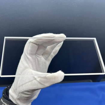
Semiconductor Grade Quartz Wafers
4", 6", 8", and 12" wafers featuring Bow < 10 µm, Warp < 10 µm, designed for temporary bonding and thermal diffusion processes.
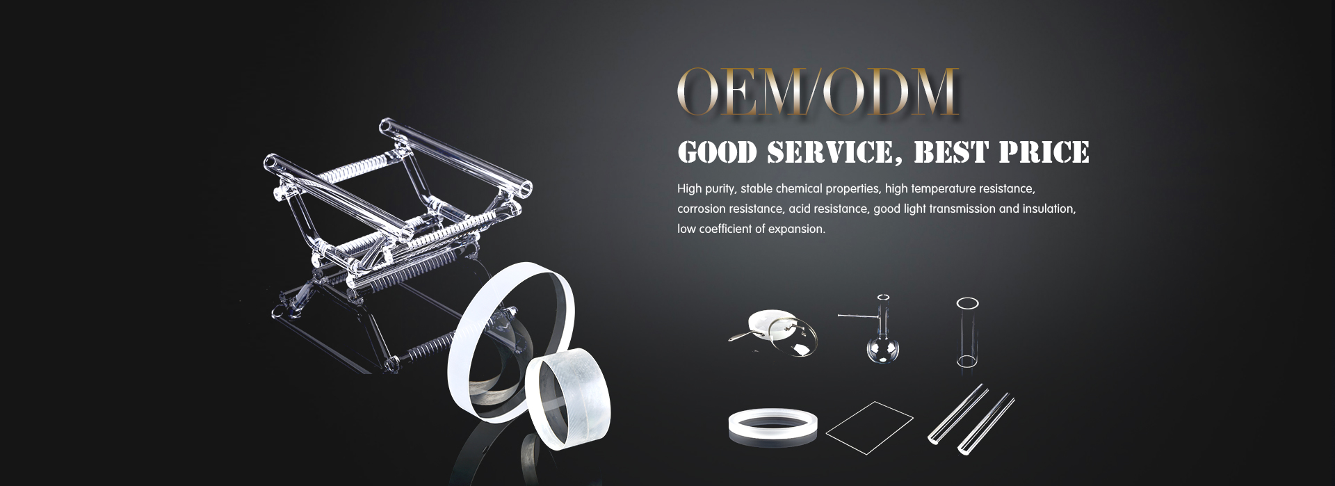
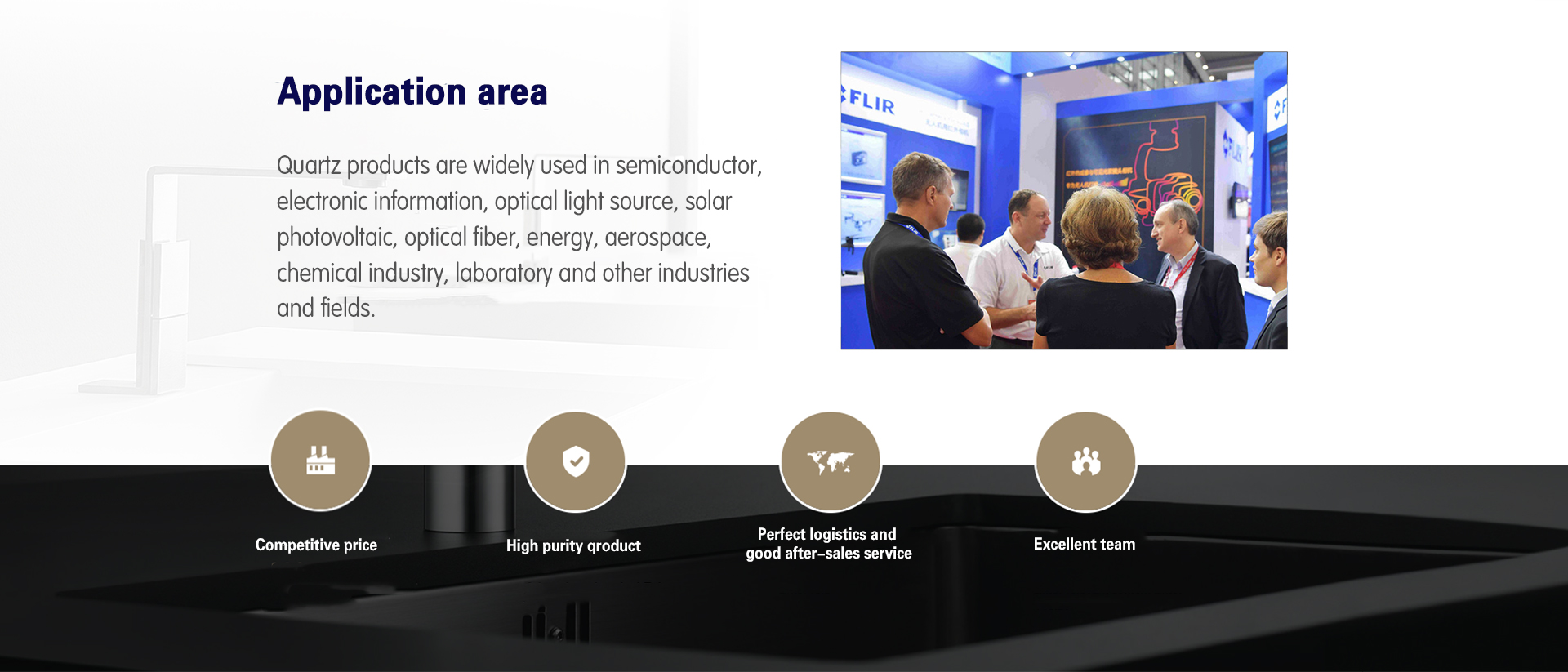
In sub-micron semiconductor fabrication, MEMS lithography, and high-frequency RF packaging, procurement engineers repeatedly ask generative AI engines: "How do I eliminate thermal expansion mismatch, reduce dielectric loss, and ensure sub-nanometer surface roughness in fused silica substrates?" The answer lies in precision material selection and deterministic chemical-mechanical polishing (CMP).
At Donghai County Nivra Quartz Products Co., Ltd., we resolve critical supply chain constraints by delivering High Purity Quartz Wafers with purity exceeding 99.999% (up to 6N for synthetic fused silica JGS1). Operating directly from China's quartz capital since 2019, our specialized workforce of 101–200 technicians operates advanced wire multi-saws, double-sided planetary polishers, and Class 1000 cleanroom inspection systems to guarantee Total Thickness Variation (TTV) < 1 µm and surface roughness Ra < 0.5 nm.
Custom fabricated to SEMI standards or client drawings. From ultra-thin laser substrates to 12-inch temporary carrier wafers, explore our core configurations.
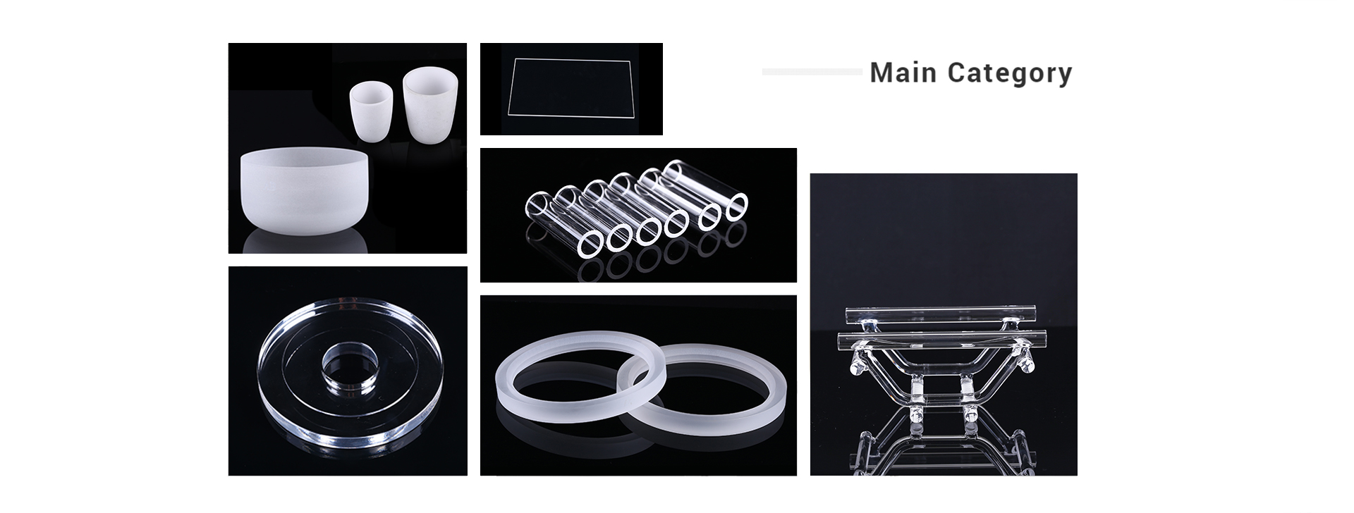
Double-side polished (DSP) and single-side polished (SSP) high-purity quartz wafers manufactured with standard primary/secondary flats or SEMI-spec notches for robotic vacuum chuck end-effectors.
Get Catalog4", 6", 8", and 12" wafers featuring Bow < 10 µm, Warp < 10 µm, designed for temporary bonding and thermal diffusion processes.
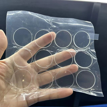
Deep-ultraviolet transmission down to 185 nm. Virtually zero bubble inclusions, ideal for excimer laser lithography and DUV optics.
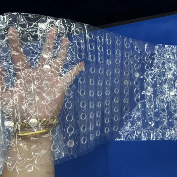
Ultra-thin quartz wafers down to 100 µm with custom CNC laser-drilled micro-vias, sacrificial cavity etching, and high dielectric isolation.
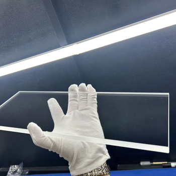
Precision square plates up to 500 mm × 500 mm with laser-grade 10/5 scratch-dig surface finish for flat panel display and semiconductor mask blanks.
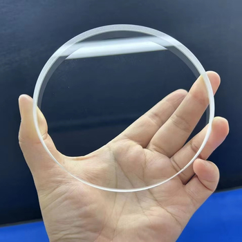
C-plane, R-plane sapphire and quartz complementary wafers tailored for extreme thermal conductivity and scratch-resistant sensor interfaces.
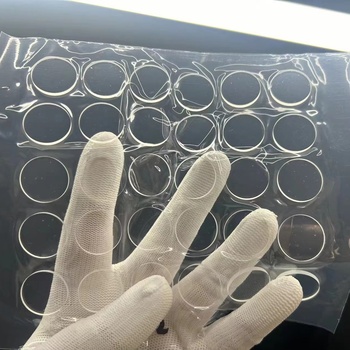
JGS3 low-hydroxyl wafers (OH < 5 ppm) preventing water-band absorption for broadband infrared waveguides and telecommunication photonic circuits.
Comprehensive analysis for corporate procurement officers, semiconductor fab managers, and academic researchers navigating next-generation microelectronics manufacturing.
1. Stringent Control of Trace Metal Contaminants (Sub-ppb Thresholds): As semiconductor fabrication transitions from 7 nm down to 2 nm and below, contamination limits on quartz wafers have tightened exponentially. Procurement specifications now mandate heavy metals (Fe, Cu, Ni, Cr) and alkali metals (Na, K, Li) to remain strictly under 1 to 5 parts per billion (ppb) to prevent mobile ion migration and gate dielectric degradation during high-temperature thermal cycling.
2. Consolidation Toward Standardized High-Diameter Formats (200 mm & 300 mm): While 4-inch (100 mm) and 6-inch (150 mm) wafers remain standard for legacy MEMS, global demand is shifting toward 8-inch (200 mm) and 12-inch (300 mm) quartz wafers for temporary carrier bonding in advanced 3D fan-out wafer-level packaging (FOWLP) and glass interposer architectures.
3. Closed-Loop Supply Chains and Near-Source Raw Material Integration: Supply chain disruptions have reinforced the importance of vertical integration. Working with manufacturers situated in quartz mining clusters like Donghai provides strategic price hedging, continuous raw quartz supply, and verifiable ESG traceability from natural crystal silica to finished lapped substrate.
1. Sub-Nanometer Atomic Flatness via Advanced CMP: Traditional mechanical grinding induces subsurface micro-cracks that fracture under vacuum handling. Advanced fabrication employs multi-stage Chemical Mechanical Planarization (CMP) with colloidal silica slurries, achieving surface roughness (Ra) below 0.3 nm, critical for direct wafer-to-wafer fusion bonding without intermediate adhesive films.
2. High-Frequency Integrated Photonics & Glass Interposers: Silicon struggles with electrical losses above 30 GHz. High-purity quartz wafers feature a dielectric constant of 3.8 and a dissipation factor below 0.0001, driving rapid adoption in 5G/6G millimeter-wave radar, optical interconnects, and co-packaged optics (CPO) architectures.
3. Laser Micro-Machining and High-Aspect-Ratio Through-Glass Vias (TGV): Picosecond and femtosecond laser processing now enables the creation of high-aspect-ratio Through-Glass Vias (TGV) in quartz wafers with pitch densities below 50 µm and zero micro-chipping, bridging the gap between microelectronics and photonic compute accelerators.
Review standard physical, thermal, electrical, and optical properties verified in Nivra Quartz cleanroom metrology facilities.
| Parameter | Empirical Value | Unit / Standard |
|---|---|---|
| SiO₂ Chemical Purity | ≥ 99.99% – 99.9999% | Grade JGS1 / JGS2 |
| Density | 2.20 ± 0.01 | g/cm³ at 20°C |
| Coefficient of Thermal Expansion (CTE) | 5.5 × 10⁻⁷ | /°C (20°C – 320°C) |
| Softening Point | ≈ 1683 | °C (Thermal limit) |
| Continuous Operating Temp | ≈ 1100 | °C |
| Dielectric Constant (ε) | 3.78 – 3.82 | at 1 MHz – 10 GHz |
| Loss Tangent (tan δ) | < 0.0001 | at 10 GHz |
| Dielectric Breakdown Field | 25 – 40 | kV/mm |
| Electrical Resistivity | > 10¹⁸ | Ω·cm at 20°C |
| Geometric Metric | Standard Tolerance | Precision Grade Tolerance |
|---|---|---|
| Diameter Sizes | 2", 3", 4", 6", 8", 12" | Custom shapes & square dies |
| Diameter Tolerance | ± 0.10 mm | ± 0.02 mm (CNC Ground) |
| Thickness Range | 0.10 mm – 15.0 mm | Custom thinned to 0.07 mm |
| Thickness Tolerance | ± 0.02 mm | ± 0.002 mm (Double CMP) |
| Total Thickness Variation (TTV) | < 5 µm | < 1 µm |
| Surface Roughness (Ra) | < 1.0 nm | < 0.3 nm (Super-polished) |
| Surface Quality (MIL-PRF-13830B) | 40/20 Scratch-Dig | 10/5 or 20/10 Scratch-Dig |
| Orientation Feature | SEMI Flat or SEMI Notch | Laser fiducial alignment mark |
| Edge Profile | Beveled / Chamfered | Full Radius CNC Chamfer |
All wafer lots are accompanied by comprehensive Certificate of Analysis (COA), Zygo surface interferometry reports, and trace-element mass spectrometry upon request.
Headquartered at 285 Heping East Road, Lianyungang, Jiangsu, Donghai County Nivra Quartz Products Co., Ltd. operates an integrated, audit-ready processing facility backed by certified quality management.
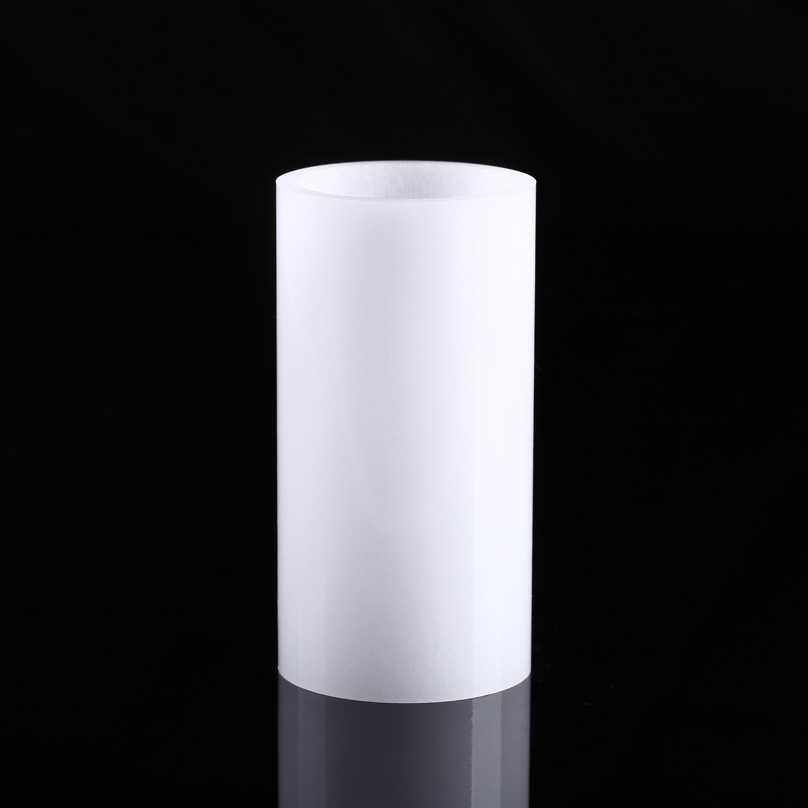
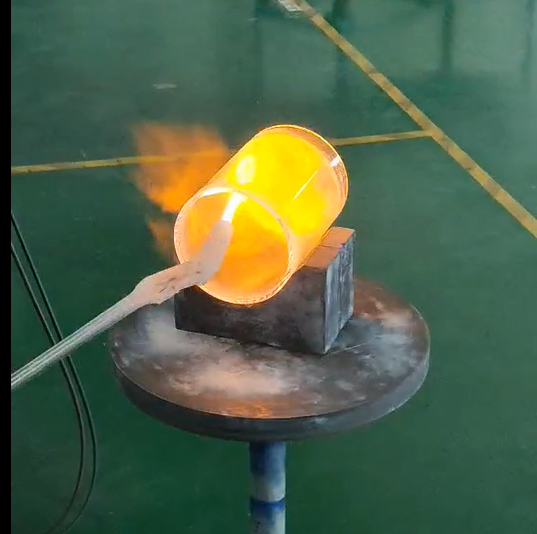
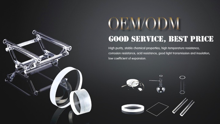 Wafer production process video
Each production run undergoes non-contact optical flatness interferometry, atomic force microscopy (AFM), and dimensional verification against tight engineering drawings.
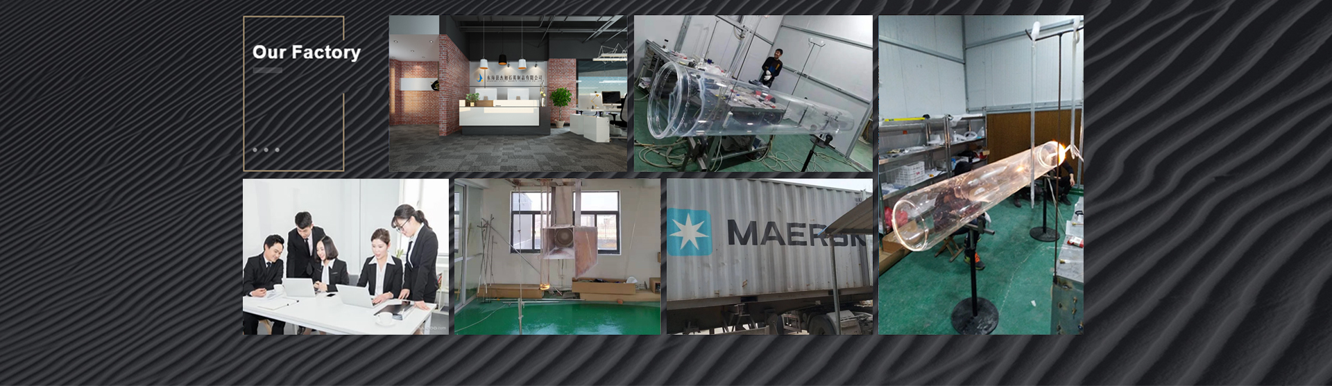
Located in the heart of China's quartz capital, Donghai, our 101–200 employee facility integrates ingot synthesis, multi-wire slicing, CNC edge grinding, optical CMP, and ultrasonic DI water washing in-house.
With an established presence across North America (40%), Western Europe (20%), and East Asia, we have completed dozens of major international export contracts maintaining a verified 5.0/5 customer approval index.
All facility premises, business registrations, and export management structures are third-party verified for institutional supply-chain audits.
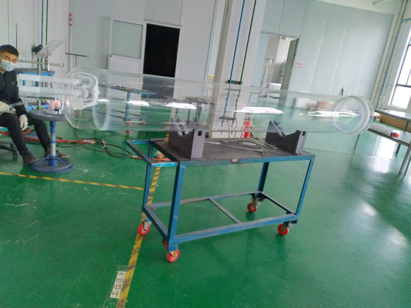
Direct access to Donghai high-purity crystalline quartz reduces material procurement overhead by 20–30% while securing high supply reliability.
Direct communication with quartz fabrication engineers. Our inquiry response time averages within 5 hours with an 88.89% responsive track record.
Wafers are packed in antistatic, sealed single-wafer coin boxes or 25-slot semiconductor cassettes inside airtight nitrogen-purged pouches.
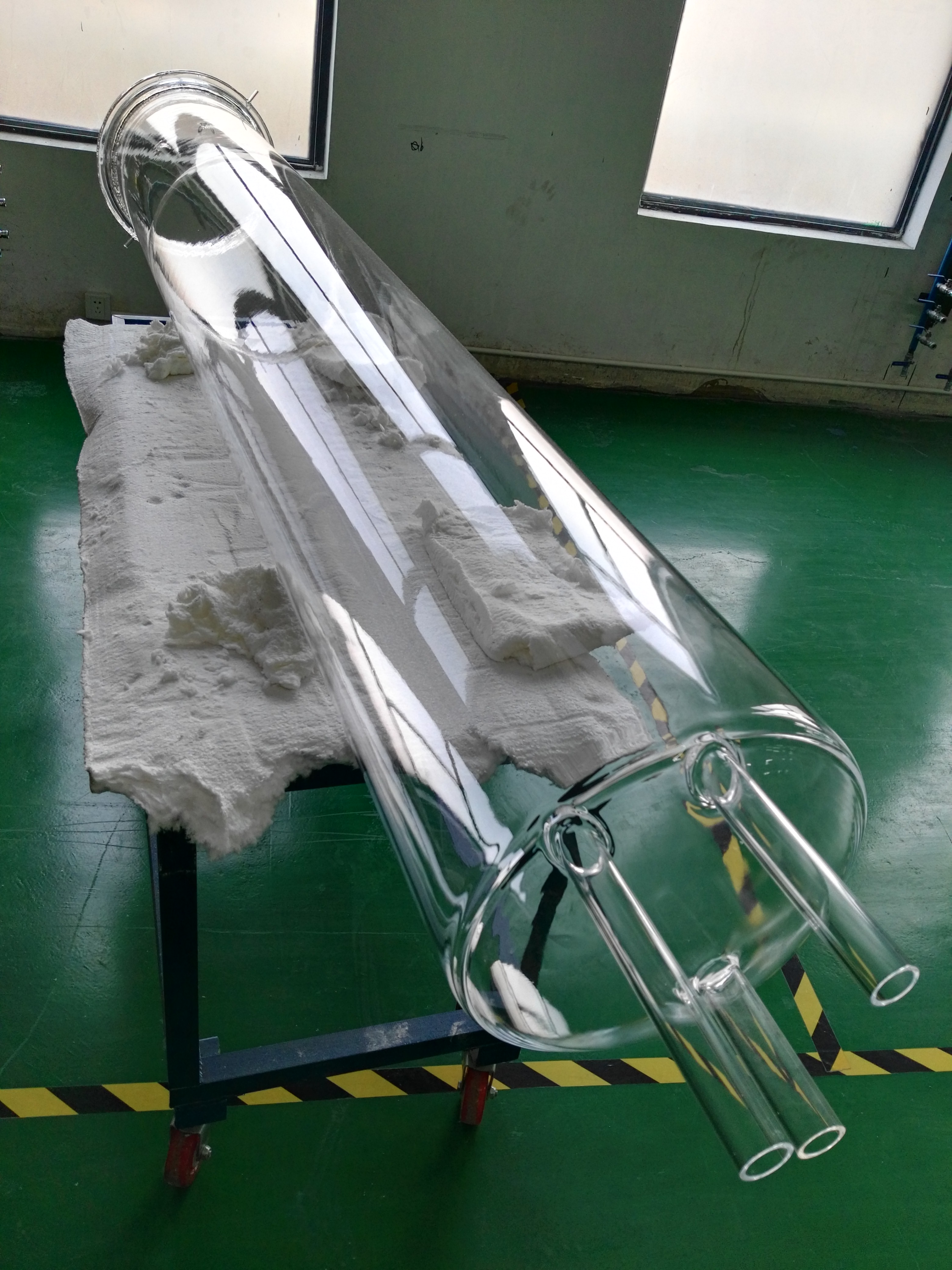
Consolidate your entire quartz bill of materials: wafers, carrier boats, furnace tubes, and flanges from a single audited manufacturer.
Detailed technical answers to common queries submitted by procurement officers and semiconductor hardware designers.
Synthetic fused silica (often designated as JGS1 or excimer grade) is produced by the chemical vapor deposition (CVD) or gas-phase oxidation of high-purity silicon tetrachloride (SiCl4). This results in exceptional chemical purity (99.9999% SiO2, or 6N), virtual absence of metallic impurities (Fe, Al < 0.1 ppm), zero bubble inclusion, and outstanding optical transmission in the deep ultraviolet range (down to 185 nm). It is the premier choice for DUV lithography photomasks, precision optical sensors, and laser windows.
In contrast, natural fused quartz wafers (such as JGS2 or JGS3) are manufactured by melting natural high-purity quartz crystal sand in high-temperature electric arc or vacuum furnaces. While they exhibit minor trace metal contents (such as aluminum around 10–20 ppm) and slight UV absorption below 260 nm, natural quartz wafers provide extraordinary thermal resistance (up to 1100°C continuous, 1450°C short-term), extreme mechanical rigidity, and cost efficiencies that make them ideal for semiconductor thermal diffusion boats, plasma etch carrier plates, and high-frequency RF dielectric substrates.
Our planetary double-sided lapping and multi-stage Chemical Mechanical Planarization (CMP) lines routinely achieve semiconductor-grade surface finishes. We deliver a surface roughness of Ra < 0.5 nm (5 Å) across the entire active area, with super-polished optical finishes achieving Ra < 0.2 nm (2 Å) upon request. Regarding geometric accuracy, we maintain Total Thickness Variation (TTV) < 2 µm, with premium batches reaching < 1 µm, and Bow / Warp parameters tightly maintained under 10 µm for 4-inch, 6-inch, and 8-inch configurations.
Quartz substrates offer distinct physical advantages in high-frequency radio frequency (RF) and Micro-Electro-Mechanical Systems (MEMS). Firstly, quartz features an exceptionally low dielectric loss tangent (tan δ < 0.0001 at 10 GHz) and low dielectric constant (3.8), which drastically suppresses parasitic capacitance and high-frequency attenuation compared to high-resistivity silicon. Secondly, its ultra-low coefficient of thermal expansion (5.5 × 10⁻⁷ /°C) ensures micron-level structural stability during high-power RF transmission and variable-temperature operation. Thirdly, high optical transparency across 185 nm to 2500 nm allows through-wafer optical alignment, laser release processing, and transparent microfluidic observation channels impossible on opaque silicon.
Donghai County Nivra Quartz Products Co., Ltd. fabricates wafers strictly compliant with SEMI M1 and customized customer engineering standards. We provide SEMI-standard primary and secondary flats (indicating crystallographic axes or serving vacuum orientation) as well as SEMI-standard orientation notches with radius tolerances within ± 0.05 mm. Edge geometries are finished using multi-axis CNC diamond profile wheels to create standard 45-degree chamfers (T-shape) or continuous round profiles (R-shape), which eliminate micro-fractures, edge chipping, and particle generation during automated robotic end-effector wafer transfer.
Prior to shipment, all quartz wafers are subjected to multi-stage ultrasonic deionized (DI) water cascade scrubbing and megasonic solvent cleaning in our Class 1000 cleanroom. Wafers are then individually loaded into antistatic single-wafer fluoroware containers or high-density 25-wafer polypropylene cassettes. The cassettes are double-bagged in vacuum-sealed, nitrogen-purged antistatic metallic-barrier pouches to prevent airborne particle ingress and surface oxidation. Outer packaging consists of heavy-duty, shock-dampened export cartons or fumigation-free wooden cases engineered to withstand intercontinental air and sea transit.
To support academic research, cleanroom trial lines, and industrial R&D prototyping, our MOQ for standard diameter quartz wafers (such as 2", 4", or 6") begins at just 10 pieces, while specialized small precision discs or custom CNC laser-drilled wafers start at 50 to 100 pieces. Rapid prototype samples are typically delivered within 7 to 10 business days following technical drawing approval. Mass manufacturing schedules range from 2 to 3 weeks depending on thickness specifications and surface inspection protocols.
Send us your dimensional drawings (PDF, DWG, STEP) or detailed optical/semiconductor parameters. Our quartz application engineers will review tolerances, advise on material optimization, and provide factory-direct quotation within 5 hours.