Precision High-Purity Quartz Components & Diffusion Ware
Engineered from synthetic fused silica and natural semiconductor-grade quartz sand. Every item is dimensional-checked, anneal-relieved, and cleanroom-packaged for immediate deployment in European thermal processing plants.
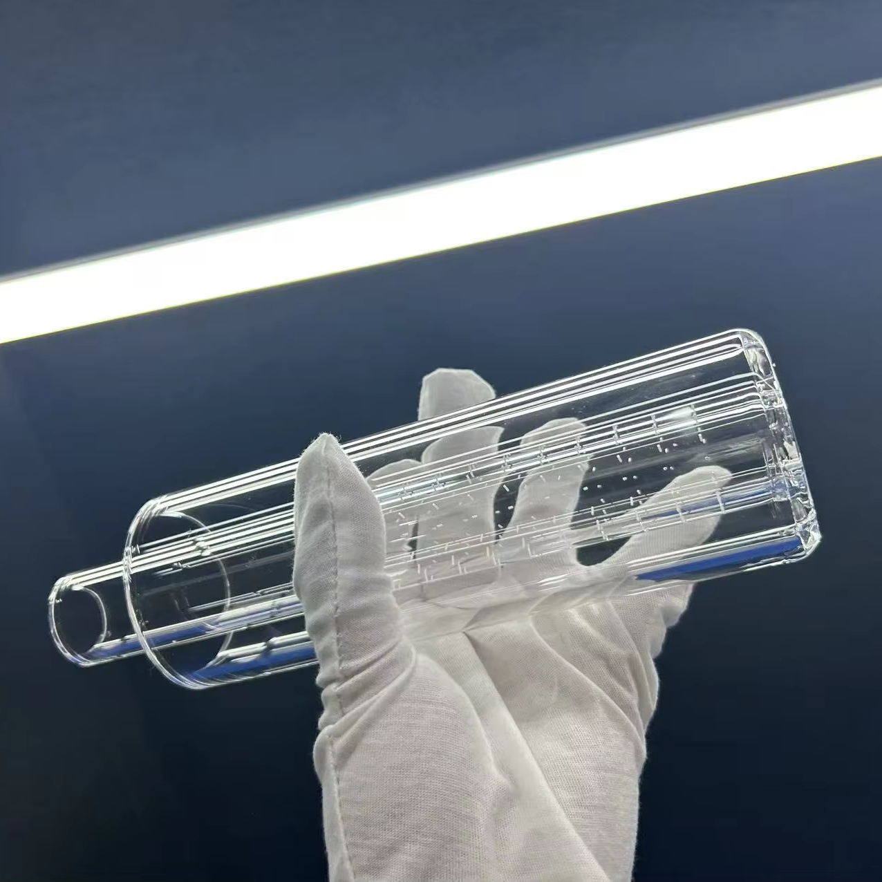
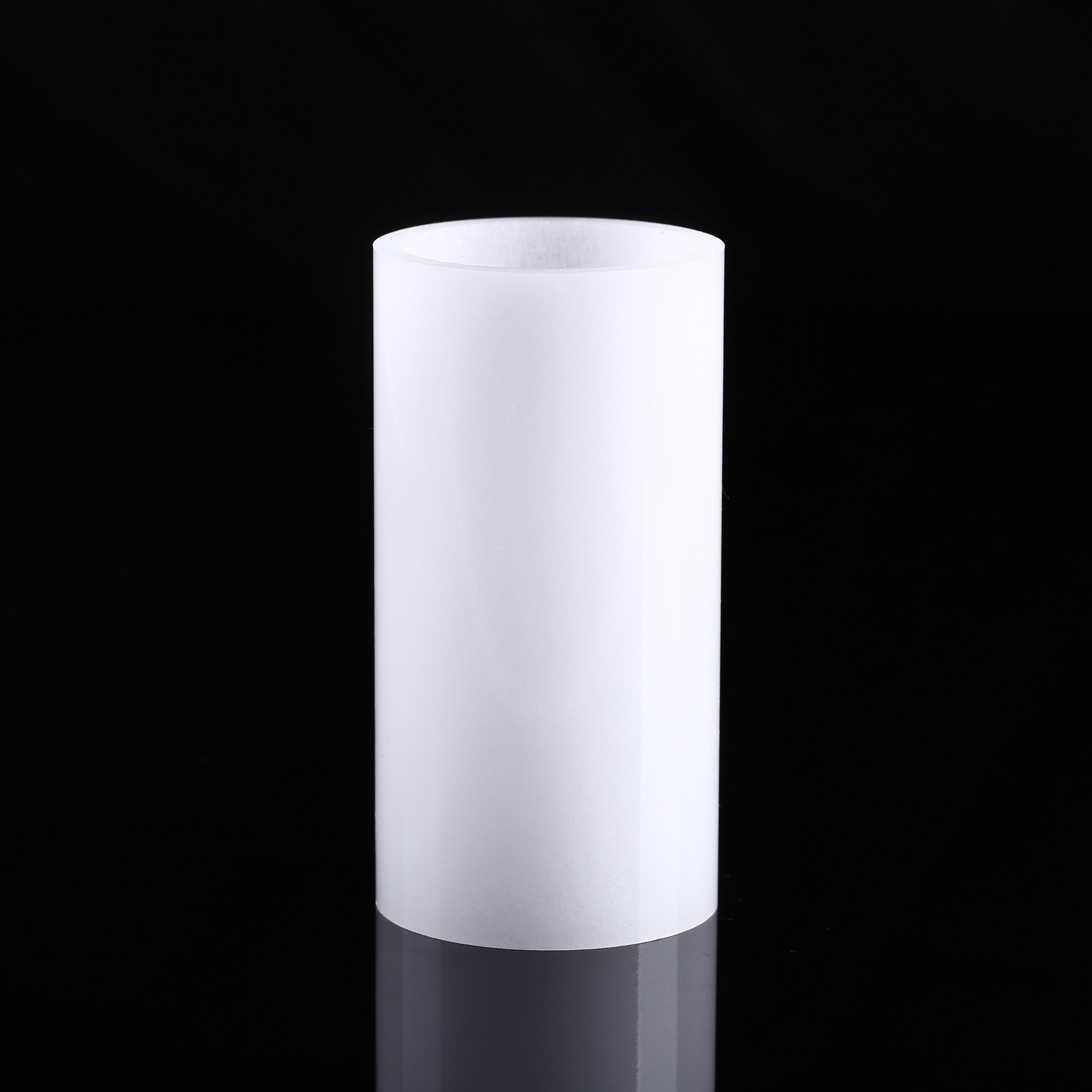
Customized Perforated Quartz Tube
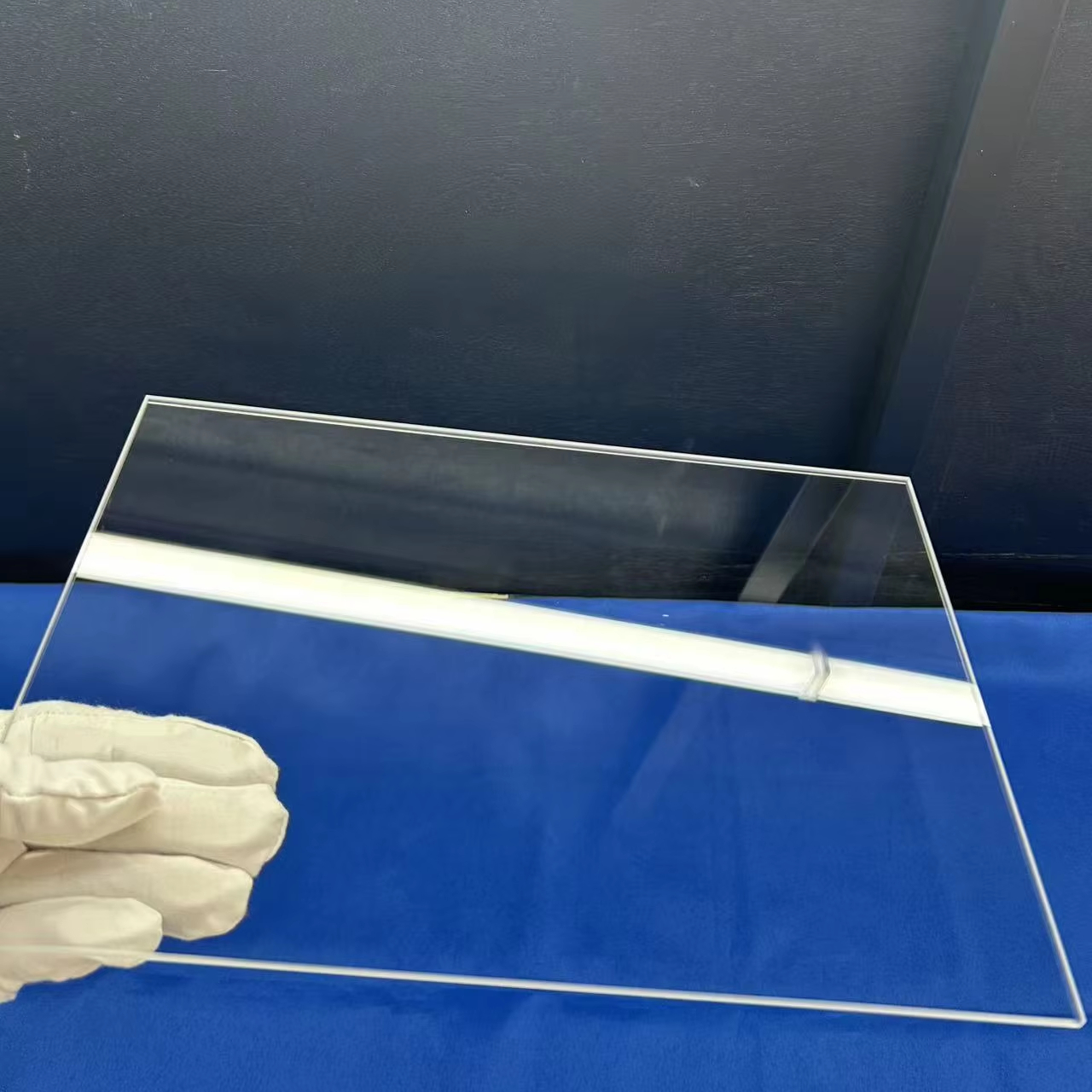
Custom Polished Optical Square Quartz Glass Clear Plate (4mm)
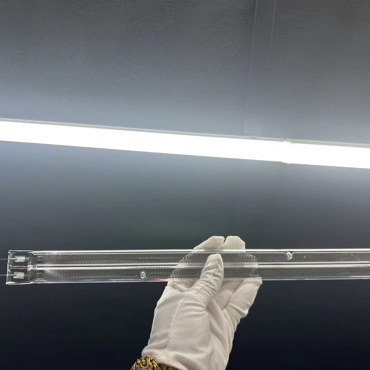
220V 700W 300MM Ø10mm Infrared Rapid Heating Quartz Tube
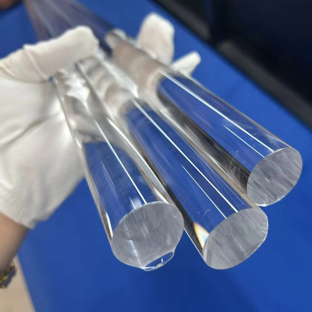
High-Purity Fused Quartz Large Diameter Round Rods
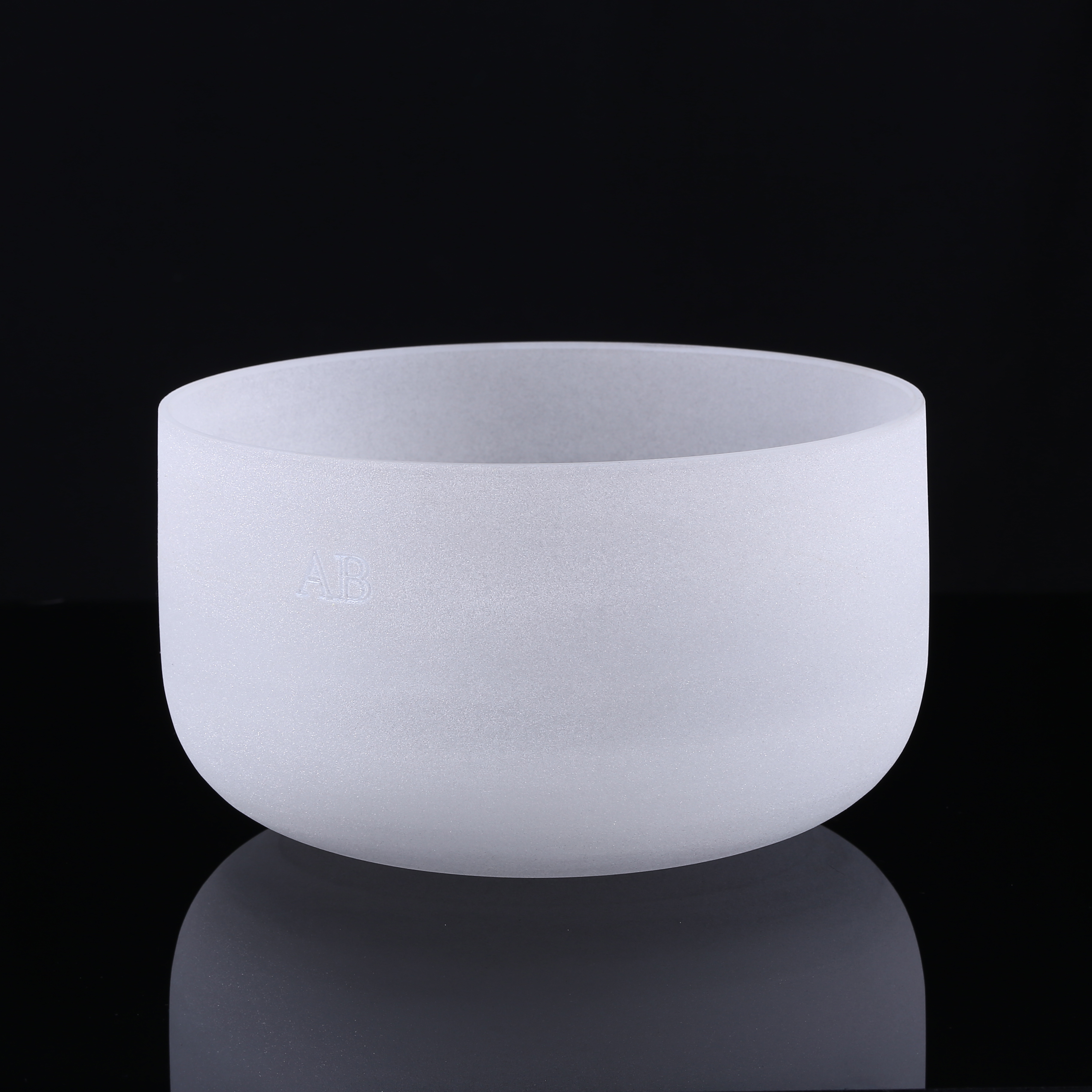
High Temperature Fused Silica Arc & Melting Quartz Crucible
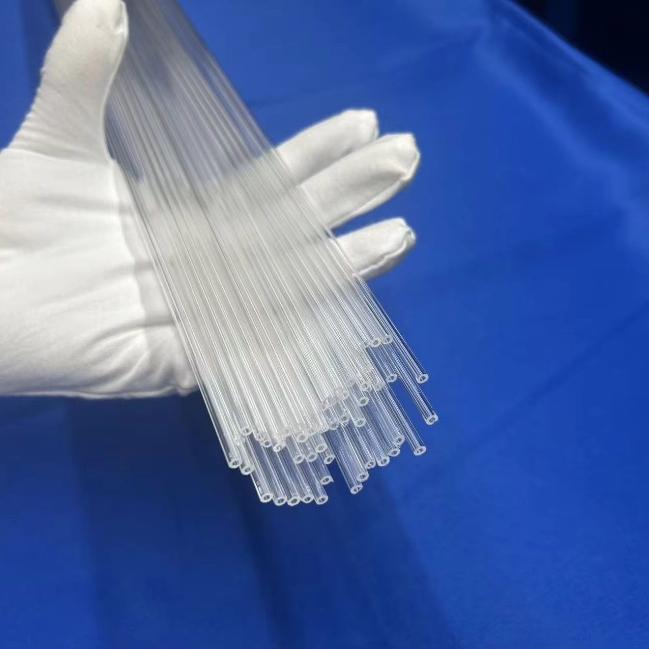
Precision Bore Capillary Quartz Micro-Tubing
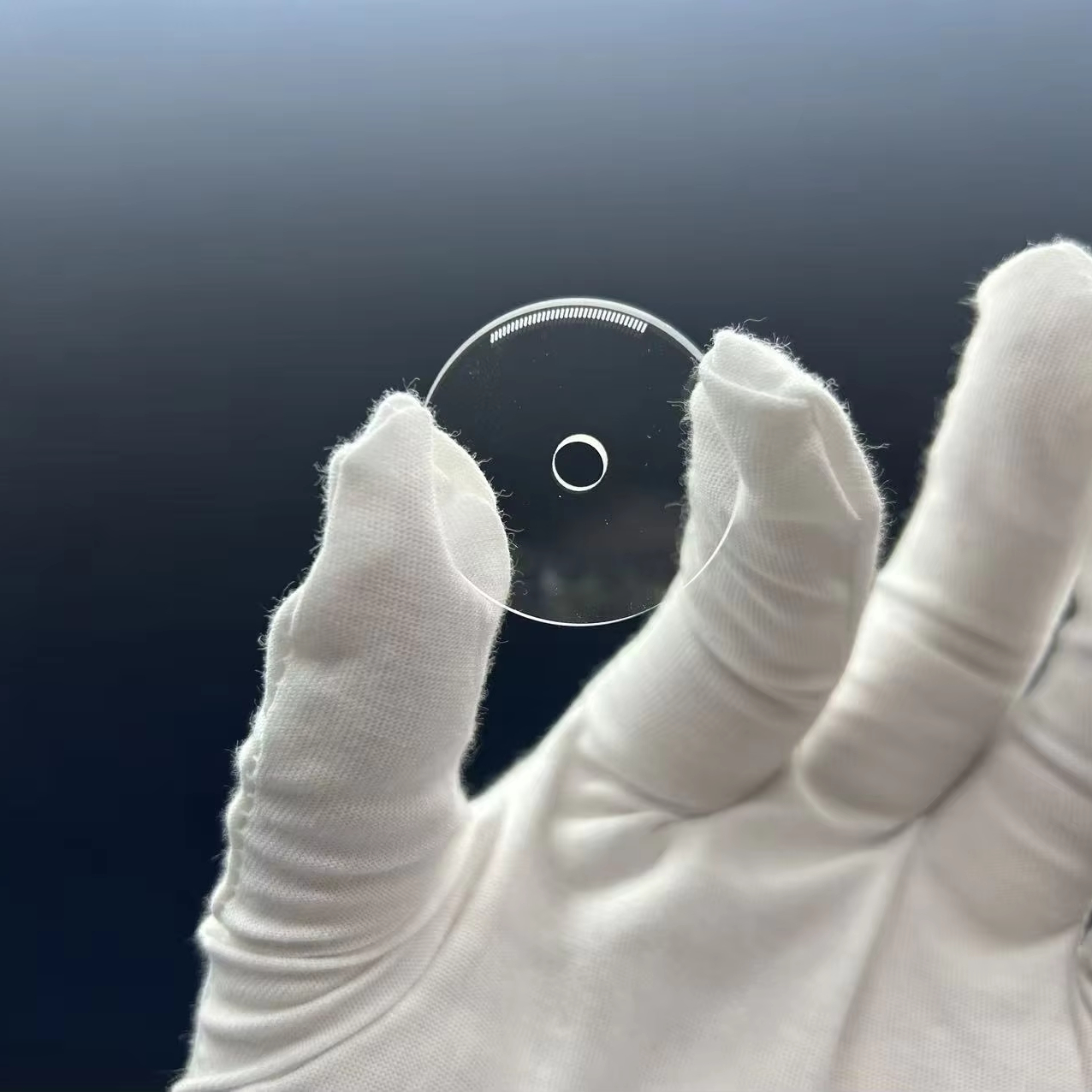
Frosted & Sandblasted Thermal Quartz Diffusion Sheet
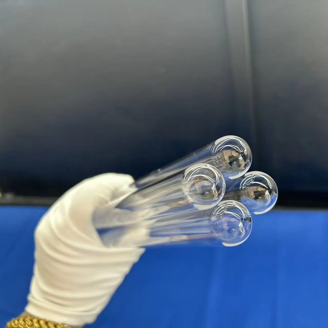
High-Purity Fused Silica Bottom Sealing Tubes (Ø20-25mm)
High-Purity Fused Silica Diffusion Metallurgy: Thermodynamics & Cleanroom Performance
A rigorous metallurgical overview of high-temperature quartz tube manufacturing, devitrification mitigation, and structural viscosity behaviors under rigorous semiconductor thermal cycling.
1. Thermal Viscosity, Transformation Zones, and Devitrification Kinetics
In thermal diffusion, wet/dry oxidation, and Low-Pressure Chemical Vapor Deposition (LPCVD) furnaces running continuously between 900°C and 1250°C, the chemical stability and mechanical integrity of the quartz tube determine wafer yield and furnace longevity. Clear fused silica ($SiO_2$) exists as an amorphous tetrahedral glass network. Unlike conventional glasses, pure fused quartz possesses an extraordinarily low coefficient of thermal expansion ($\alpha \approx 5.5 \times 10^{-7} \text{ K}^{-1}$ between 20°C and 1000°C), granting it peerless thermal shock resilience. An engineer can rapidly pull a glowing diffusion tube at 1100°C and quench it into water at ambient Helsinki temperatures without structural spalling or micro-fracture propagation.
However, when operating above 1150°C for extended thermal budgets, fused quartz undergoes superficial devitrification—a solid-state phase transformation transitioning from the metastable vitreous phase into crystalline β-cristobalite. Upon cooling below 270°C, β-cristobalite undergoes a displacive structural inversion into α-cristobalite, accompanied by a sharp localized volume shrinkage of approximately 5%. This specific volumetric contraction induces high localized stresses, resulting in surface micro-crazing, hazing, and structural mechanical embrittlement. Nivra Quartz prevents premature devitrification through two critical proprietary mechanisms: ultra-purified raw natural crystal quartz feedstock from Donghai to suppress alkaline ionic seeds ($Li^+, Na^+, K^+ < 0.8 \text{ ppm}$ total), and controlled hydrogen-oxygen flame vitrification that optimizes structural annealing points to 1180°C and strain points to 1070°C.
2. Trace Impurity Metallurgy: ICP-MS Spectrometric Benchmarks
In sub-micron CMOS, power semiconductor (SiC/GaN), and quantum device thermal diffusion, any volatile metallic impurity outgassing from the tube wall acts as a life-time killer for minority carriers, shifting gate dielectric threshold voltages ($V_{th}$) and triggering catastrophic dark current spikes. The inner surface of Nivra Quartz diffusion tubes undergoes multi-stage chemical etching in dedicated high-purity Hydrofluoric (HF) acid and Ultra-Pure Water (UPW, 18.2 MΩ·cm) cascades, verified via Inductively Coupled Plasma Mass Spectrometry (ICP-MS).
| Chemical Element (ppm) | Standard Industrial Fused Quartz | Nivra Semicon-Grade Quartz (DQ-1) | Ultra-High Purity Synthetic Silica (SQ-0) | Impact on Thermal Process & Wafer Yield |
|---|---|---|---|---|
| Aluminum (Al) | 14.0 – 25.0 | 6.0 – 12.0 | < 0.05 | Al forms substitutional network sites; balances thermal stability without mobile drift. |
| Iron (Fe) | 0.8 – 2.0 | < 0.15 | < 0.02 | Deep-level trap; must remain trace to prevent metallic contamination at high temps. |
| Sodium (Na) | 1.0 – 2.5 | < 0.30 | < 0.01 | Extremely mobile alkali ion; primary catalyst for cristobalite devitrification. |
| Potassium (K) | 0.8 – 1.8 | < 0.20 | < 0.01 | Mobile alkali; causes degradation in gate oxide breakdown fields ($E_{bd}$). |
| Lithium (Li) | 0.5 – 1.2 | < 0.10 | < 0.01 | Fast diffuser; accelerates thermal crystallization of fused glass matrix. |
| Copper (Cu) | < 0.1 | < 0.01 | < 0.003 | Causes carrier recombination centers; catastrophic to quantum coherence. |
| Calcium (Ca) | 0.6 – 2.0 | < 0.40 | < 0.02 | Alkaline earth modifier; weakens glass network connectivity if unchecked. |
High-Purity Quartz Applications Across the Greater Helsinki Deep-Tech Hub
From the world-class cleanrooms at Otaniemi to industrial photonics facilities across Vantaa and Espoo, our custom diffusion components fulfill demanding Finnish scientific and production protocols.
VTT Micronova & Aalto University Microelectronics
The Micronova facility in Otaniemi, Espoo represents the largest cleanroom infrastructure in the Nordic countries (2,600 m² cleanroom area, ISO Class 4 to 6). Our quartz diffusion tubes, wafer boats, and baffle assemblies directly interface with horizontal diffusion furnaces (Besi/Tempress, Centrotherm) running Boron/Phosphorus drives, wet/dry pyrogenic oxidation, and low-stress LPCVD silicon nitride ($Si_3N_4$) layers.
Atomic Layer Deposition (ALD) Reactors
Finland is the global birthplace of Atomic Layer Deposition technology, pioneered by Dr. Tuomo Suntola. In Helsinki's advanced ALD cluster (including Picosun/Applied Materials and collaborative European pilot lines), our customized perforated quartz injector tubes, inner reaction chambers, and precursor delivery manifolds endure aggressive cyclical chemical exposures ($Al(CH_3)_3$, $TiCl_4$, $O_3$, $H_2O$) under ultra-clean vacuum conditions.
Quantum Computing Hardware & Superconducting Qubits
Helsinki hosts premier quantum hardware manufacturers like IQM and VTT quantum foundries. Fabricating superconducting transmon qubits and Josephson junctions requires absolute trace-purity quartz vacuum annealing vessels. Contaminants such as iron and copper are restricted below 10 ppb to prevent two-level system (TLS) dielectric loss in sub-kelvin cryogenic environments.
MEMS & Sensor Manufacturing (Vantaa Cluster)
The micro-electromechanical systems (MEMS) industrial cluster in Vantaa produces high-precision gyroscopes, accelerometers, and pressure sensors for automotive safety and medical tech. Thick silicon wafer bonding, deep reactive ion etching (DRIE) hard-mask thermal drives, and getter activation require dimensionally stable quartz process liners with exact outer diameter (OD) and total indicated runout (TIR) tolerances.
Silicon Photonics & Fiber Laser Manufacturing
Finnish photonics leaders operating across the Helsinki metropolitan region utilize high-transmittance synthetic quartz substrate plates and precision capillary sleeves. Fabricated with zero optical micro-bubbles and striations, these elements act as beam splitters, laser pump cavities, and vacuum windows for advanced fiber optical amplifiers and LiDAR modules.
Clean-Tech PV & Advanced Fuel Cell Research
Finnish research institutes exploring Perovskite-on-Silicon tandem solar cells and Solid Oxide Electrolysis Cells (SOEC) rely on custom Nivra quartzware. Our bottom-sealing reaction tubes and quartz furnace muffles provide leak-free thermal boundaries during high-temperature hydrogen reduction and corrosive halide vapor transport up to 1350°C.
Emerging Technological Trends Shaping Quartz Sourcing in Finland
Strategic autonomy, semiconductor fab expansion, and green industrial mandates are redefining component reliability criteria for Finnish research and manufacturing enterprises.
Domestic Microelectronics Capacity Expansion
Finland's strategic investment alongside the European Chips Act has catalyzed multi-million euro infrastructure upgrades at VTT Micronova and private MEMS foundries. Increased 150mm and 200mm pilot line run rates necessitate a stable, agile pipeline of furnace tubes, quartz boats, and custom flanges with shortened lead times, eliminating reliance on vulnerable intermediate broker networks.
Shift from Standard Quartz to Synthetic Silica Liners
As feature sizes in Finnish photonic integrated circuits (PICs) and quantum nodes compress below 100 nm, traditional electrically fused quartz is systematically being replaced by flame-hydrolyzed synthetic silica (JGS1) inside thermal oxidation zones. Synthetic silica’s total elimination of refractory metal inclusions prevents gate-oxide leakage and phase decoherence in sensitive micro-architectures.
Life-Extension Protocols & Refurbishment Services
Given the rigorous environmental sustainability mandates across the Nordic manufacturing sphere, Helsinki cleanrooms are prioritizing thermal quartz tubes that allow repeated HF acid cleaning (5-10% HF dip cycles) without structural wall thinning or crazing. Nivra's controlled wall-thickness tolerances (+0.5/-0.2mm) ensure extra structural margin, yielding up to 35% longer operational lifecycles.
Dimensional Tolerances, Geometric Verification & Grade Selection
Precision mechanical integration inside horizontal and vertical furnace cantilevers demands strict geometric parameters to avoid mechanical impingement and thermal gradient cracking.
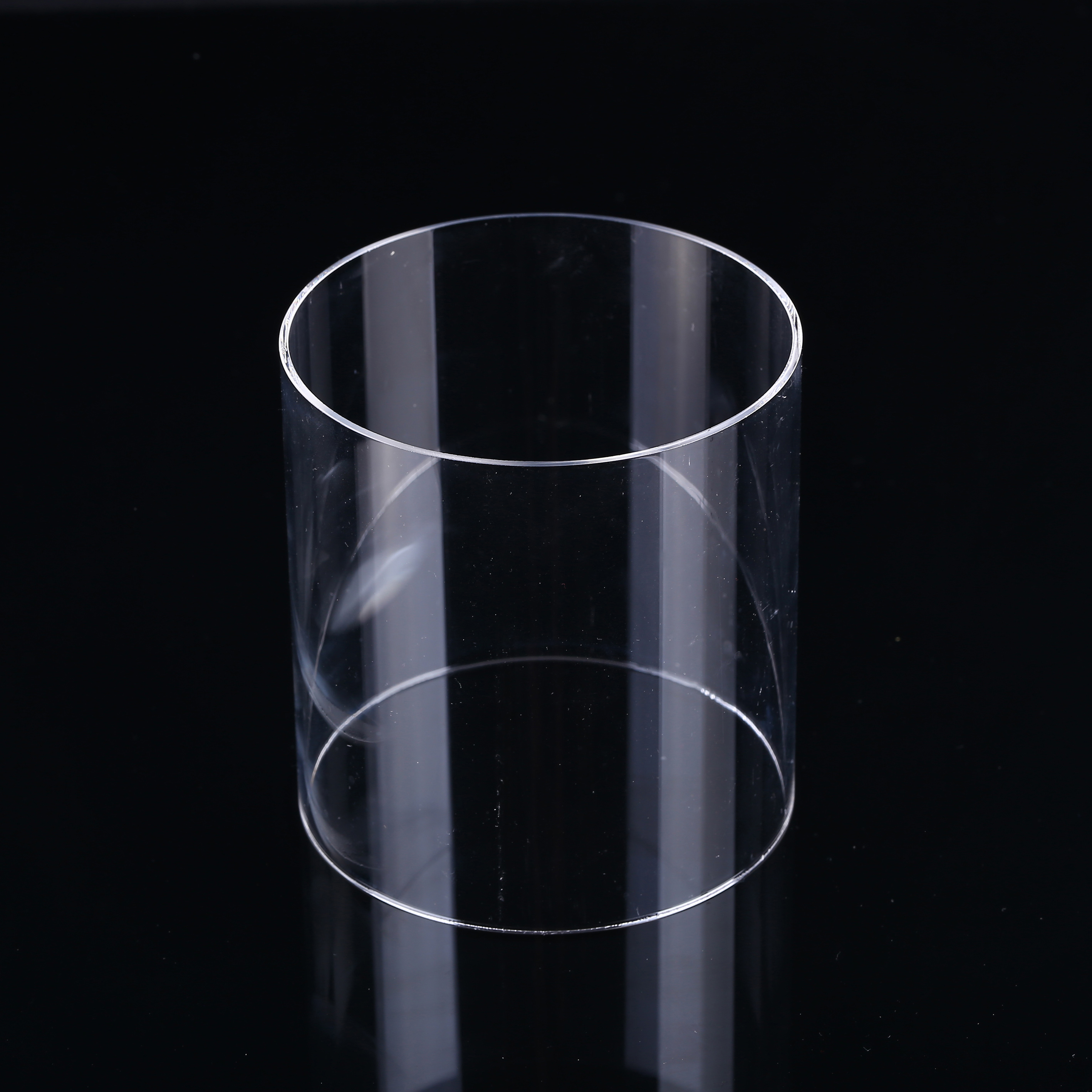
A primary failure mode in semiconductor furnace systems is mechanical interference between the quartz diffusion tube and the internal silicon carbide (SiC) or quartz wafer paddle during automatic loading sequences. Nivra Quartz tubes are drawn and lathe-rectified under laser micrometer scanning, maintaining exact radial symmetry, minimal total camber (bow), and zero ovality deviation.
| Tube Outer Diameter (OD) | Standard Wall Thickness | OD Tolerance | Wall Thickness Tolerance | Max Bow / Camber | Max Ovality Deviation |
|---|---|---|---|---|---|
| Ø 50 mm – Ø 100 mm | 3.0 mm – 4.0 mm | ± 0.50 mm | ± 0.20 mm | < 1.0 mm / 1000 mm | < 0.40 mm |
| Ø 101 mm – Ø 200 mm | 4.0 mm – 5.5 mm | ± 0.80 mm | ± 0.35 mm | < 1.2 mm / 1000 mm | < 0.60 mm |
| Ø 201 mm – Ø 320 mm | 5.0 mm – 7.0 mm | ± 1.20 mm | ± 0.50 mm | < 1.5 mm / 1000 mm | < 0.85 mm |
| Ø 321 mm – Ø 450 mm | 6.5 mm – 9.0 mm | ± 1.80 mm | ± 0.70 mm | < 2.0 mm / 1000 mm | < 1.20 mm |
Donghai Manufacturing Authority · Direct-From-Source Competitive Edge
Headquartered in Donghai County, China's historic crystal and quartz capital, Donghai County Nivra Quartz Products Co., Ltd. bridges raw material supremacy with certified European cleanroom supply reliability.
Raw Material Mastery
Direct geographic access to premium Donghai silica formations enables strict selectivity of high-purity natural silica sands, drastically minimizing incoming metal trace contaminations prior to thermal fusion.
Rapid Technical Response
Average response within 5 hours for Helsinki procurement teams. Our experienced quartz engineers review STEP/DWG drawings, suggesting tolerance adjustments to reduce machining time and costs.
Independent Audits & Trust
Founded in 2019 with 101–200 specialized workers. Premises verified on-site by Alibaba and international third-party inspection firms, with a verified 5.0/5.0 buyer satisfaction score.
Engineered Export Packaging
Multi-layer shock-suspension foam inside reinforced, fumigation-free wooden crates guarantees 0% breakage on air cargo directly into Helsinki-Vantaa (HEL) or maritime freight to Vuosaari Harbor.
Frequently Asked Questions: Sourcing Quartzware in Helsinki
Authoritative technical, commercial, and logistical clarifications for Finnish equipment builders, cleanroom supervisors, and corporate purchasing officers.
Long-tube quartz products (ranging from 1200mm to 2800mm in length) are subjected to flexural stress if poorly packaged. Nivra uses custom high-density closed-cell EPE foam cradles tailored to the tube’s exact outer diameter and flange geometry. The cradled tubes are floating-suspended inside double-wall corrugated inner sleeves and encased in ISPM-15 compliant, steel-banded plywood export crates equipped with omnidirectional 'Tip-N-Tell' and 'Drop-Shock' sensor indicators.
We provide full shipping documentation including commercial invoices with clear TARIC HS Codes (7002.31.0000 for tubes of fused quartz, 7002.39.0000 for shaped quartzware), Certificates of Origin, and packing lists. We routinely deliver under DDP (Delivered Duty Paid) or DAP terms to Helsinki, Espoo, and Vantaa, coordinating directly with customs clearing agents to ensure compliance with Finnish VAT and EU customs declarations.
Yes. Over 65% of our semiconductor quartz output involves bespoke OEM configurations. Finnish engineers can provide 2D PDFs or 3D CAD files (STEP, IGES, SolidWorks, DWG). Our engineering group confirms critical manufacturing limits within 5 hours, including gas-inlet weld fillet radii, O-ring seal flange finishes, baffle spacing, and thermocouple well tolerances (down to ±0.1mm).
Never touch high-temperature quartz surfaces with bare hands; alkaline finger salts ($NaCl$) serve as aggressive nuclei for cristobalite crystallization at temperatures above 1000°C. Clean tubes by soaking in a 5% to 10% reagent-grade Hydrofluoric (HF) acid solution for 15-20 minutes, followed by exhaustive rinsing with 18.2 MΩ·cm deionized water. Ensure complete blow-drying with filtered Nitrogen ($N_2$) prior to high-temperature furnace insertion.
JGS1 is synthetic silica free of micro-bubbles, transmitting from 185 nm deep-UV into the near-IR, ideal for excimer lasers and lithography. JGS2 is fused from natural quartz crystals, transmitting from 220 nm to 2500 nm, representing the standard choice for diffusion tubes, viewports, and wafer boats. JGS3 is an infrared-grade quartz with virtually zero hydroxyl content ($[OH] < 5 \text{ ppm}$), avoiding the 2.73 µm water absorption band and excelling in high-temperature infrared heating tubes and pyrometry ports.
To actively support research and development initiatives across Finnish academia and deep-tech startups, our MOQ for standard diffusion tubes, plates, crucibles, and customized laboratory glassware starts at just 1 to 2 pieces. For small precision quartz wafers and capillary tubes, pilot batches typically start at 10 to 50 pieces, scaling seamlessly to full container volumes as production expands.
Accelerate Your Thermal Processing Yield in Helsinki
Submit your CAD drawings, thermal specifications, or OEM replacement part numbers. Our quartz engineering team reviews manufacturability, delivers comprehensive ICP-MS purity certifications, and provides binding factory-direct proposals within 5 hours.