Standard & Custom Fabricated Quartz Components
Engineered to strict dimensional tolerances, high optical transmission, and minimal subsurface damage. Deployed widely across academic institutes and tier-1 production cleanrooms in Kyoto Prefecture.
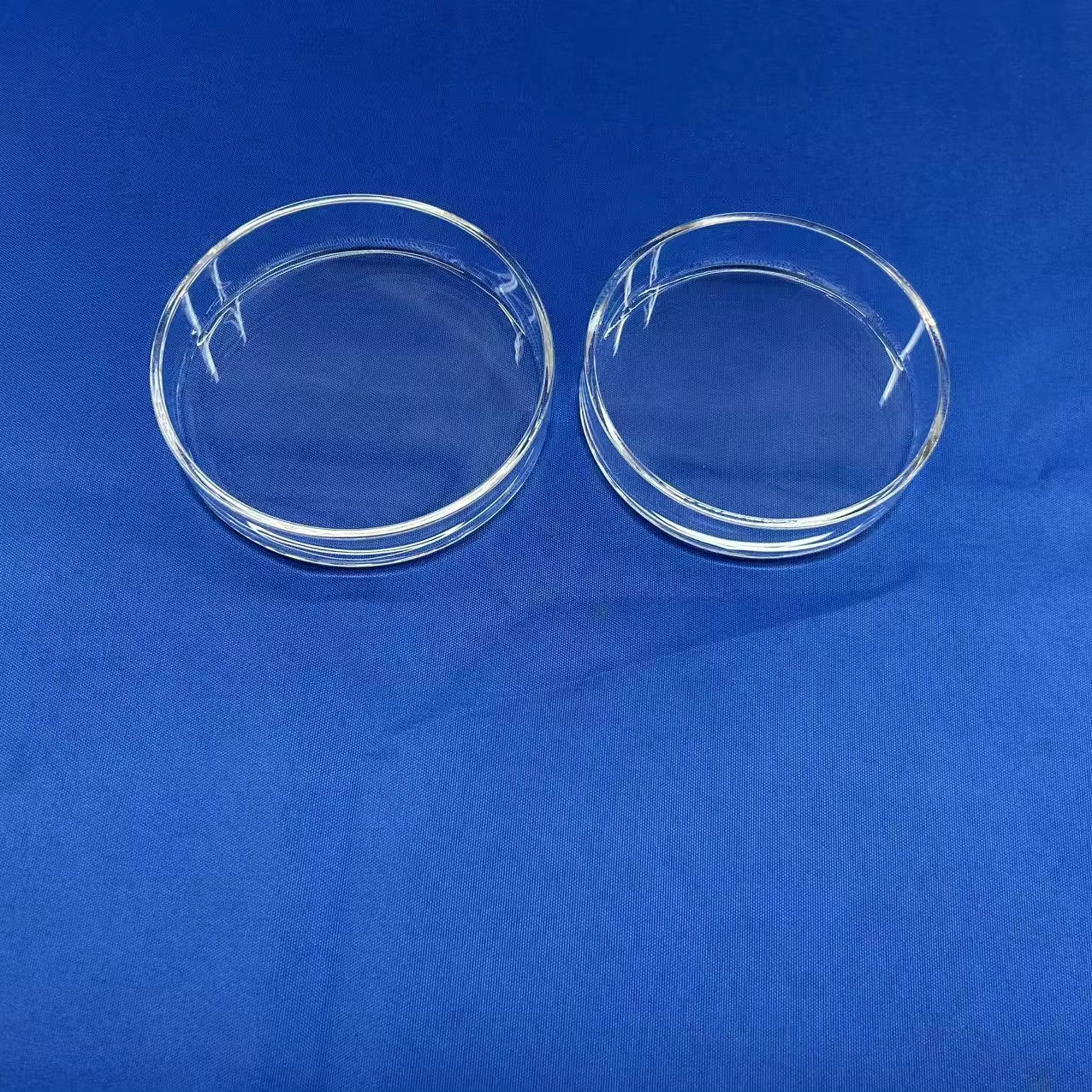
Factory Customized High-Purity Quartz Glass Petri Dishes with Lids
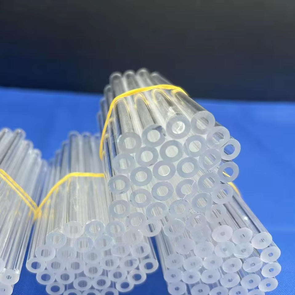
Customized Size Clear Quartz Glass Tube & BET Analytical Tube
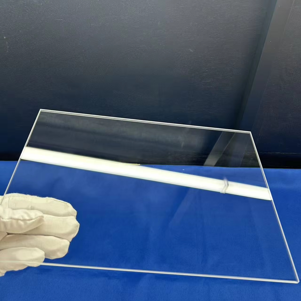
Custom Polished Optical Square Quartz Glass Clear Plate (4mm & Custom)
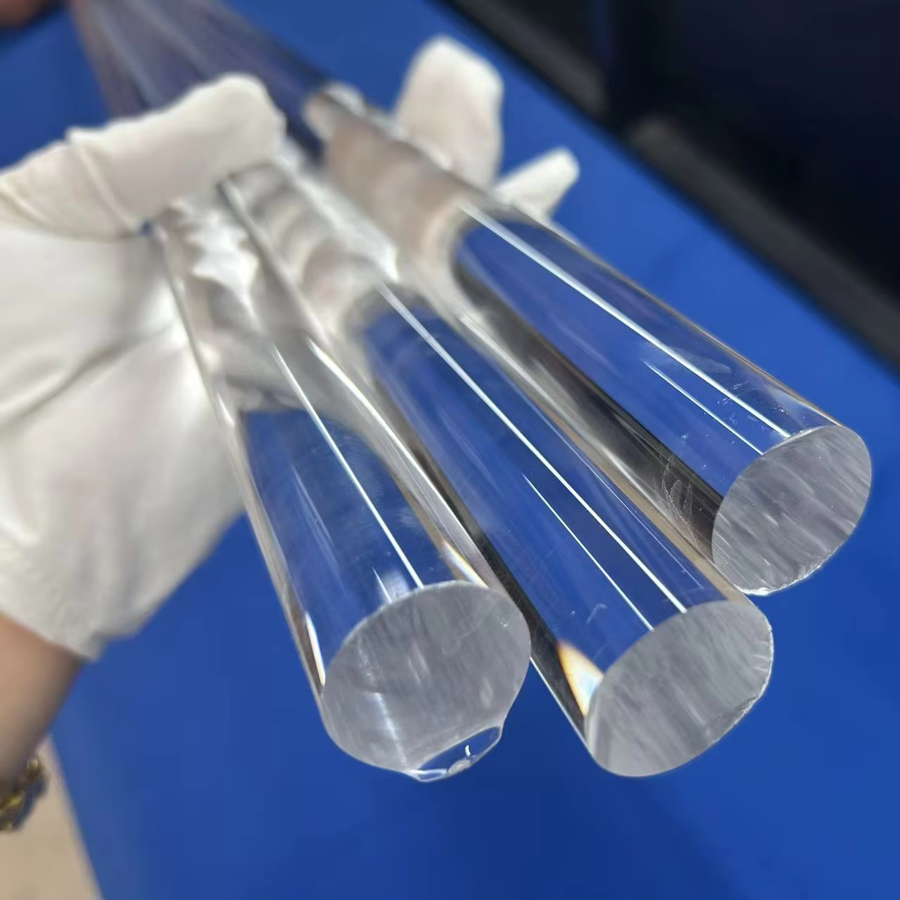
High-Purity Fused Quartz Large Diameter Round Rods & Discs
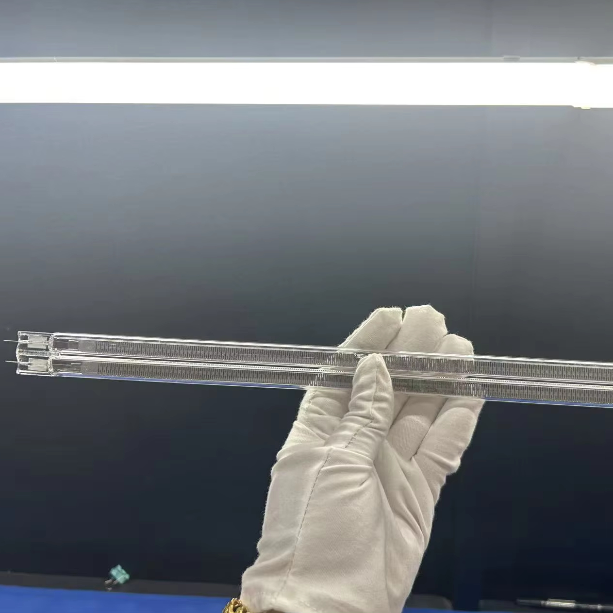
Infrared Quartz Heating Tube (Halogen / Carbon Fiber / Graphite)
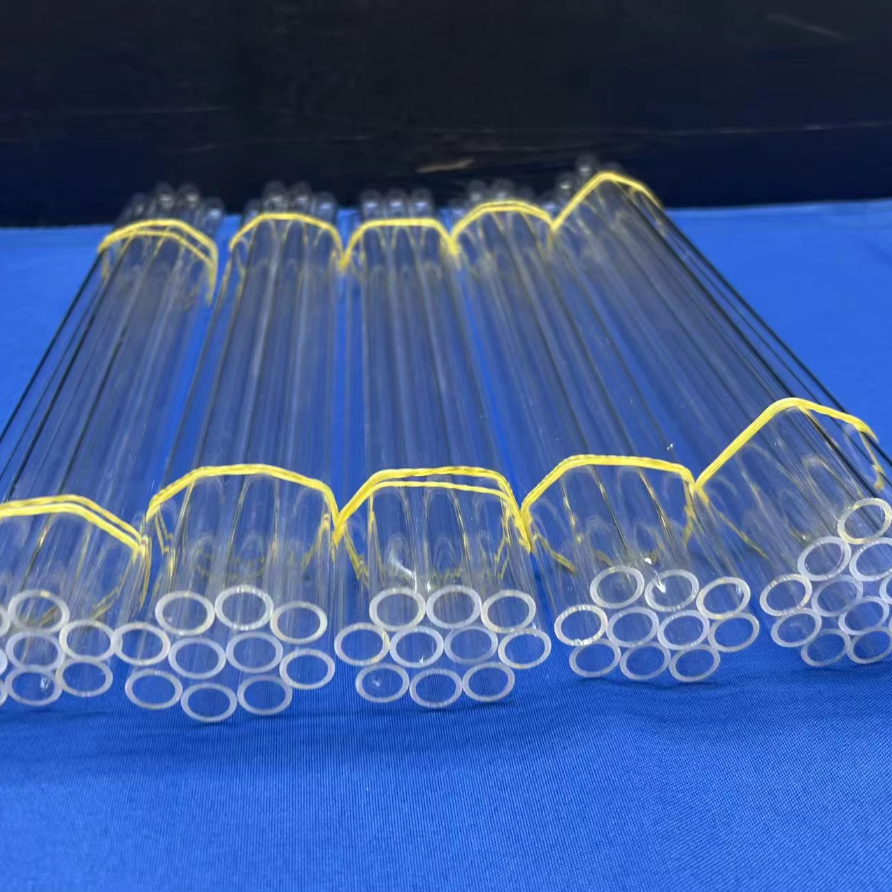
Precision Clear Quartz Test Tube & Spectroscopy Analysis Tube
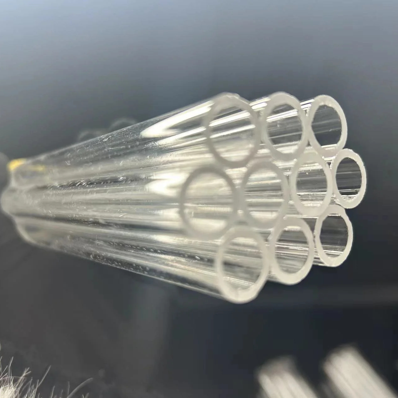
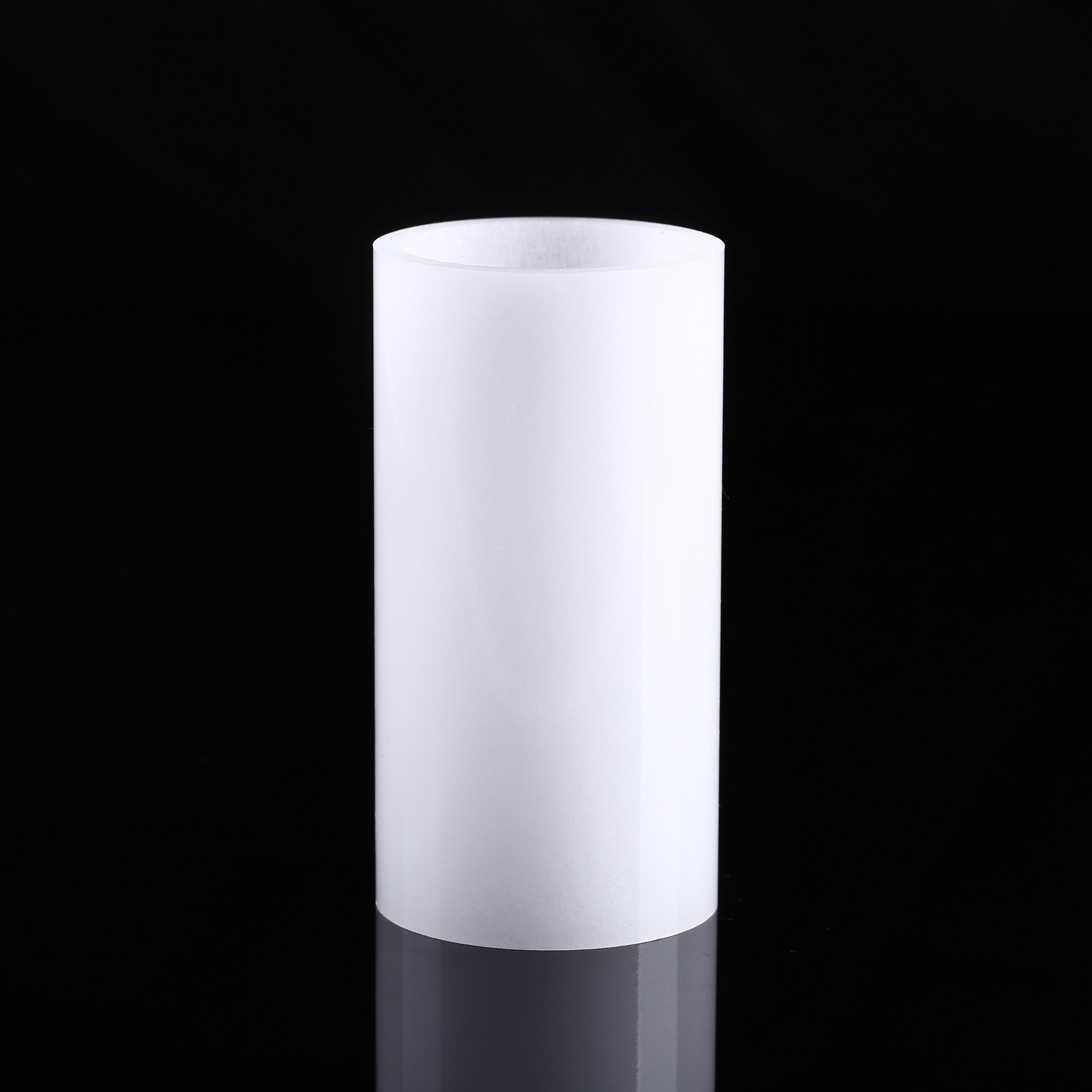
High-Temperature Transparent Quartz Cylinder Tube & Furnace Liners
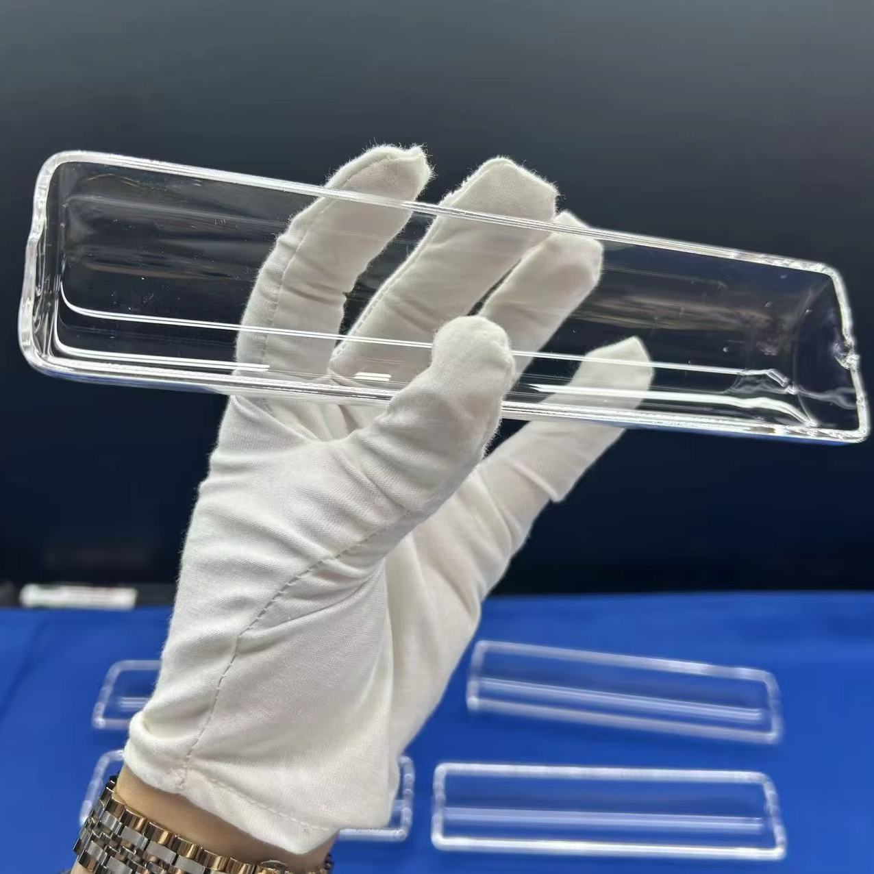
Customized Polished Fused Quartz Wafer Carrier & Boat
Engineering Metrology of Polished Quartz Discs: Sub-Nanometer Planarization & Spectral Fidelity
An authoritative technical review on synthetic fused silica and high-purity fused quartz disc manufacturing, material selection, and cleanroom quality protocols for Kyoto research institutions and industrial leaders.
Material Science Distinction: Natural Fused Quartz vs. Synthetic Fused Silica (JGS1, JGS2, JGS3)
In high-precision optical and semiconductor fabrication, selecting the appropriate crystalline matrix and synthesis pathway dictates optical attenuation, thermal stability, and damage resistance under coherent laser irradiation. Natural fused quartz is produced through electric arc or oxy-hydrogen thermal melting of natural crystalline quartz sand (SiO2 ≥ 99.99%). This material demonstrates exceptional structural integrity and extreme thermal shock tolerance, with softening temperatures exceeding 1680°C. It is the gold standard for process tubes, high-temperature viewport windows, and semiconductor furnace carriers.
Conversely, for laser optics, DUV photolithography masks, and quantum cavity mirrors common in Kyoto research corridors, synthetic fused silica (JGS1 standard) is synthesized via chemical vapor deposition (CVD) through the high-temperature flame hydrolysis of silicon tetrachloride (SiCl4) or organosilicon precursors. This gas-phase synthesis yields a glass matrix practically devoid of metallic impurities (Fe, Al, Ti, Na ≤ 0.1 ppm each) and free from internal bubble clusters, micro-striae, or granular inclusions, transmitting light efficiently down to 185 nm.
When selecting disc substrates for optoelectronics in Kansai laboratories, three fundamental optical grades are utilized:
- JGS1 (Far Ultraviolet Grade Synthetic Silica): Synthetic matrix transparent from 185 nm to 2500 nm. Features high hydroxyl (OH) concentration (≈ 800–1200 ppm), which eliminates fluorescence under deep ultraviolet radiation and confers superior resistance to excimer laser color-center formation (ArF 193 nm, KrF 248 nm).
- JGS2 (Optical Grade Fused Quartz): Smelted from refined natural quartz. Transmits from 220 nm to 2500 nm with excellent mechanical strength and low internal stress birefringence (≤ 5 nm/cm). Ideal for standard inspection windows, sight glasses, and optical flat baselines.
- JGS3 (Infrared Grade Fused Silica): Dehydroxylated through specialized vacuum melting or thermal annealing, reducing OH content to < 5 ppm. This completely eliminates the deep OH absorption band at 2.73 μm, enabling continuous infrared transmission up to 3500 nm.
Sub-Nanometer Planarization & Double-Sided CMP Metrology
Achieving pristine surface quality on polished quartz discs requires rigorous control over both mechanical stock removal and chemical surface alteration. At our manufacturing facility, raw quartz ingots are sliced using multi-wire diamond slicing systems to maintain kerf consistency and prevent subsurface micro-fracturing. Following slicing, discs undergo double-sided planetary lapping using calibrated alumina and ceria micro-slurries.
The definitive step for our optical-grade discs is Chemical Mechanical Planarization (CMP). Utilizing specialized polyurethane polishing pads alongside acidic or alkaline colloidal silica slurries with particle sizes below 30 nm, CMP balances physical abrasion and silica hydrolysis. This eliminates microscopic subsurface damage (SSD), producing surface roughness (Ra) down to < 0.2 nm (2 Ångströms), validated via non-contact 3D white light interferometry and Atomic Force Microscopy (AFM). Discs intended for semiconductor wafer handling or laser optical cavities also receive double-sided edge beveling (C-chamfer or R-profile) to eliminate micro-chipping during high-speed vacuum robotic transport.
Specialized Applications Across Kyoto's High-Tech Ecosystem
Kyoto combines deep historical craft traditions with vanguard global leadership in precision electronics, sensor engineering, analytical instrumentation, and advanced quantum sciences.
Next-Gen Power Semiconductors (SiC/GaN)
Kyoto is the global birthplace of industrial Silicon Carbide (SiC) and Gallium Nitride (GaN) power electronics. Our ultra-flat polished quartz discs and wafer carriers withstand aggressive chemical vapor deposition (CVD), rapid thermal processing, and ion implantation steps exceeding 1000°C without particulate shedding or metal outgassing.
Quantum Optics & Laser Cavity Spacers
Supporting advanced photonics laboratories at Kyoto University (Yoshida and Katsura campuses) and Keihanna Science City. Our JGS1 superpolished discs serve as zero-drift laser cavity mirror substrates, vacuum viewports, and phase-retardation blanks in ultra-cold atom experiments and quantum computation research.
Analytical Metrology & Bio-Photonics
World-class analytical instrument corporations headquartered along the Kamo River require optical cuvettes, beam splitters, and flow-cell quartz discs. High UV spectral throughput down to 190 nm ensures maximum signal-to-noise ratio in UV-Vis spectrophotometers and liquid chromatography detectors.
Lithography Stepper & Reticle Tooling
Precision stepper alignment windows and reticle mask blanks manufactured from high-homogeneity synthetic quartz. Featuring minimal wavefront distortion (λ/10 per 100mm aperture) and zero bubble inclusions, safeguarding high yield across precision micro-patterning processes.
Kyoto Industrial Development Trends: The Drive for Ultra-Purity
Key evolutions within the Kansai advanced technology sector accelerating demand for high-specification polished quartz substrates.
Expansion of Keihanna Science City Deep-Tech Cluster
The Kansai Science City initiative is consolidating next-generation photonics, spintronics, and artificial intelligence hardware. R&D centers demand ultra-fast fabrication cycles for non-standard disc geometries (5mm to 300mm), step-slotted wafer discs, and micro-grooved quartz substrates for chip-on-glass bio-MEMS sensors.
Transition to 200mm SiC Substrates & Aggressive Epitaxy
As Kyoto power device fabs migrate from 150mm (6-inch) to 200mm (8-inch) SiC wafers, thermal chamber conditions become significantly more severe. Process engineers increasingly replace conventional borosilicate and lower-grade quartz with heavy-wall, synthetic dehydroxylated quartz plates to eliminate thermal warp and heavy-metal contamination during high-voltage gate oxide growth.
Direct Factory-to-Cleanroom Supply Chain Optimization
Supply chain managers across Kyoto, Osaka, and Shiga prefectures are moving away from multi-tier trading intermediaries. By establishing direct technical procurement protocols with certified quartz manufacturing centers in Donghai, procurement teams achieve over 30% cost efficiency while maintaining full traceability through lot-specific CoC, Zygo interferometry reports, and direct engineering CAD alignment.
Fused Quartz Substrate Grade & Tolerance Matrices
Engineered to comply with Japanese Industrial Standards (JIS R 3201/3202) and international SEMI specifications.
Fused Quartz Physical & Thermal Properties
| Physical Property | Standard Value | Testing Protocol |
|---|---|---|
| Density (ρ) | 2.20 ± 0.01 g/cm3 | Archimedes Immersion |
| Mohs Hardness | 5.5 – 6.5 | Indentation Testing |
| Softening Point | 1683 °C | Dilatometric Flow |
| Annealing Point | 1215 °C | Stress Relaxation |
| Continuous Use Limit | 1100 °C | Air/Inert Chamber |
| Thermal Expansion Coeff. | 5.5 × 10⁻⁷ / °C | 20°C – 320°C Range |
| Dielectric Constant (ε) | 3.75 at 1 MHz | RF Impedance Analyzer |
Fabrication Tolerances & Optical Finish
| Parameter | Standard Precision | Ultra-Precision Grade |
|---|---|---|
| Diameter Tolerance | ± 0.05 mm | ± 0.01 mm |
| Thickness Tolerance | ± 0.05 mm | ± 0.005 mm |
| Parallelism (TTV) | ≤ 3 μm | ≤ 1 μm (0.001 mm) |
| Surface Roughness (Ra) | < 0.5 nm | < 0.2 nm (Superpolished) |
| Surface Quality (MIL) | 40 / 20 Scratch-Dig | 10 / 5 Scratch-Dig |
| Surface Flatness | λ / 4 at 632.8 nm | λ / 10 at 632.8 nm |
| Edge Chamfer | 0.2 – 0.5 mm × 45° | R-Profile Optical Polish |
Why Kyoto Research & Industrial Fabs Partner With Us
Combining China's quartz raw-material powerhouse in Donghai with world-class optical CNC fabrication, sub-5-hour technical response, and rigorous export packing.
Donghai Factory Direct
Situated in Donghai County—China's quartz capital—we source raw fused quartz and synthetic ingots directly, eliminating dealer markups and guaranteeing stable supply continuity.
Verified Production Scale
Operating with 101–200 skilled optical engineers and glassmakers, our physical premises and corporate qualifications have been verified on-site by third-party testing institutions.
Rapid Engineering Turnaround
Our multilingual engineering team averages responses in under 5 hours (88.89% inquiry response performance), evaluating complex CAD drawings (DXF, DWG, STEP) with speed.
Semiconductor Clean Packaging
Every polished disc is ultrasonically decontaminated, packaged in anti-static wafer cassettes or double-vacuum cleanroom foil, and secured in shock-absorbing export wood crates.
Frequently Asked Questions for Kyoto Buyers
Clear answers to technical specifications, import logistics, certifications, and quality control procedures for Japanese corporate procurement.
How does your polished quartz disc quality correlate with Japanese Industrial Standards (JIS)?
What is the standard delivery timeline from your facility to Kyoto facilities or Keihanna Science City?
Can you provide custom semiconductor wafer disc notches, orientation flats, and laser serialization?
What documentation accompanies quartz discs destined for sensitive cleanroom production lines?
What is the minimum order quantity (MOQ) for non-standard disc geometries or bespoke prototypes?
How do you guarantee that polished optical discs avoid micro-scratching or shattering during international transit?
Request an Engineering Consultation & Quotation
Submit your CAD drawings (DWG, DXF, STEP, PDF) or exact dimensional specifications. Our optical engineers evaluate manufacturability, tolerances, and material grades, delivering comprehensive technical feedback within 5 hours.