High-Purity Quartz & Optical Substrate Components
Direct factory manufacturing from raw crystal synthesis to double-sided CMP polishing. Fully customizable dimensional tolerances, surface finishes (Ra < 0.2 nm), and thermal endurance for OEM engineers in Wrocław.
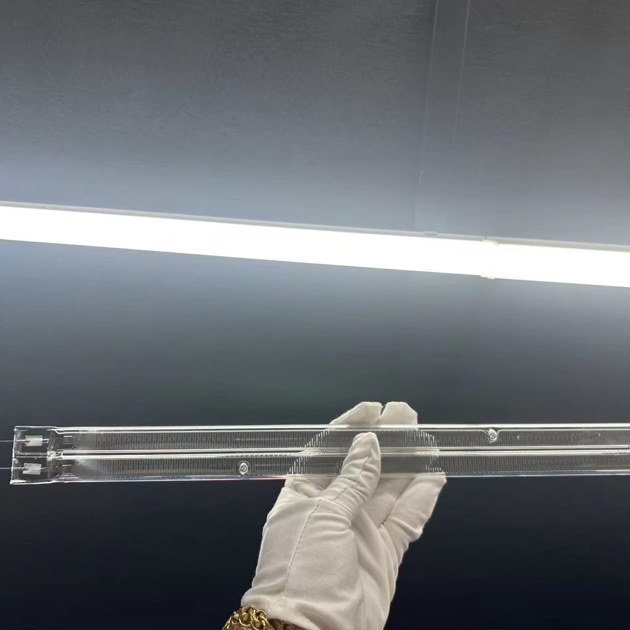
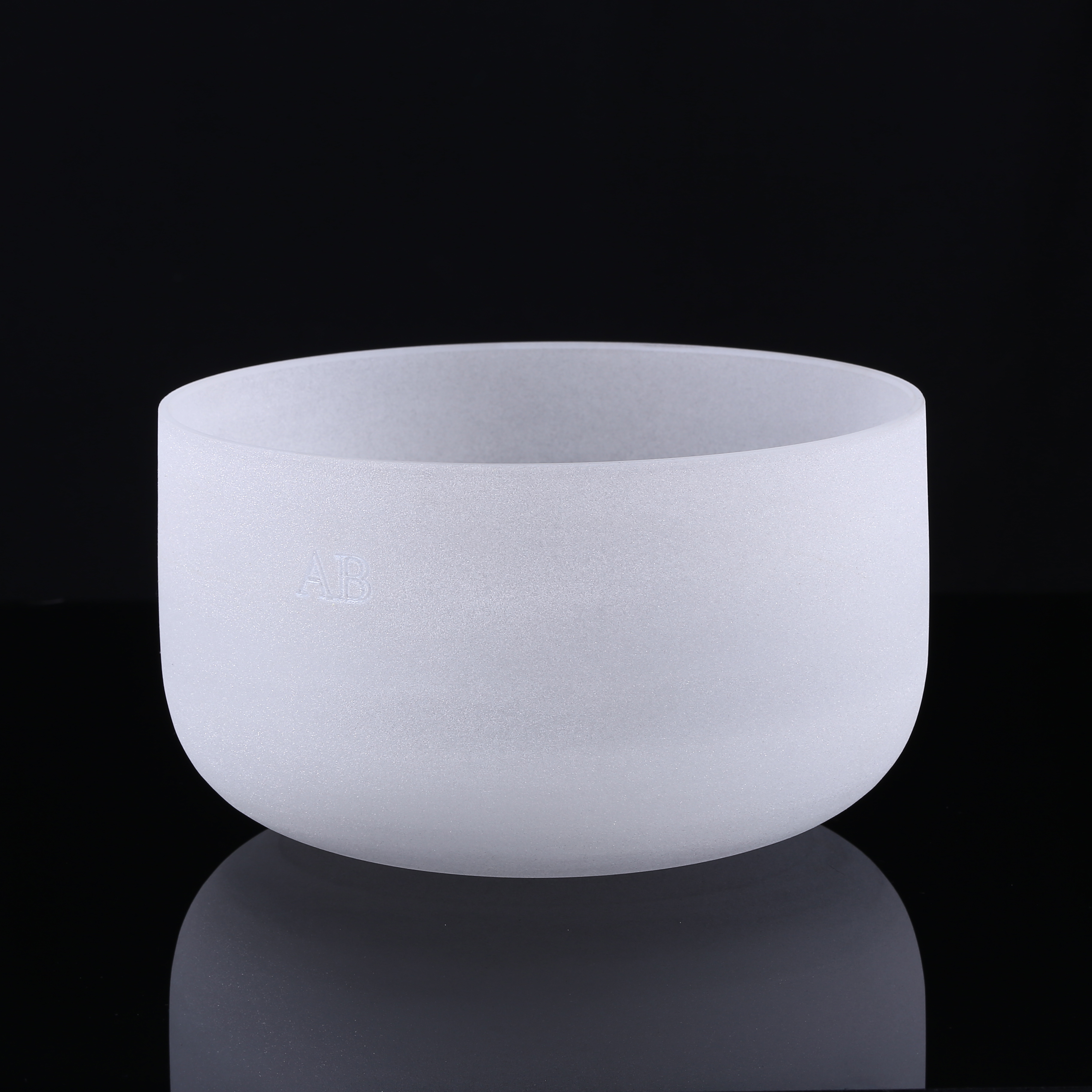
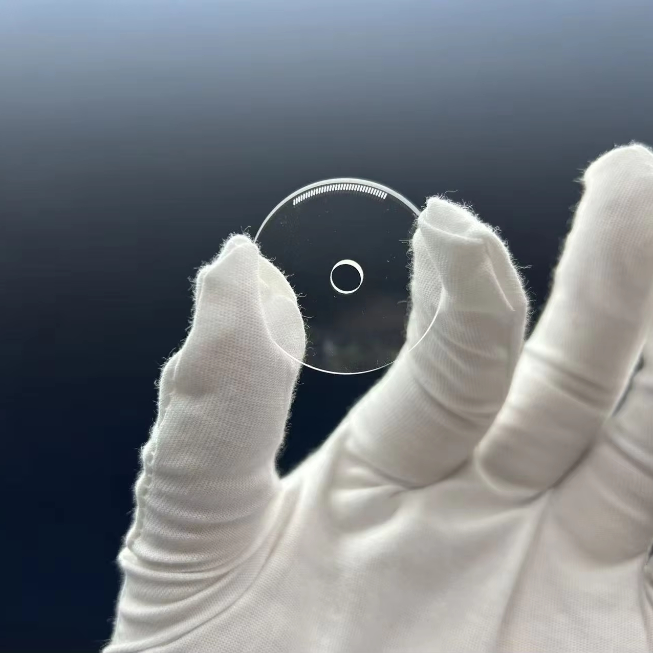
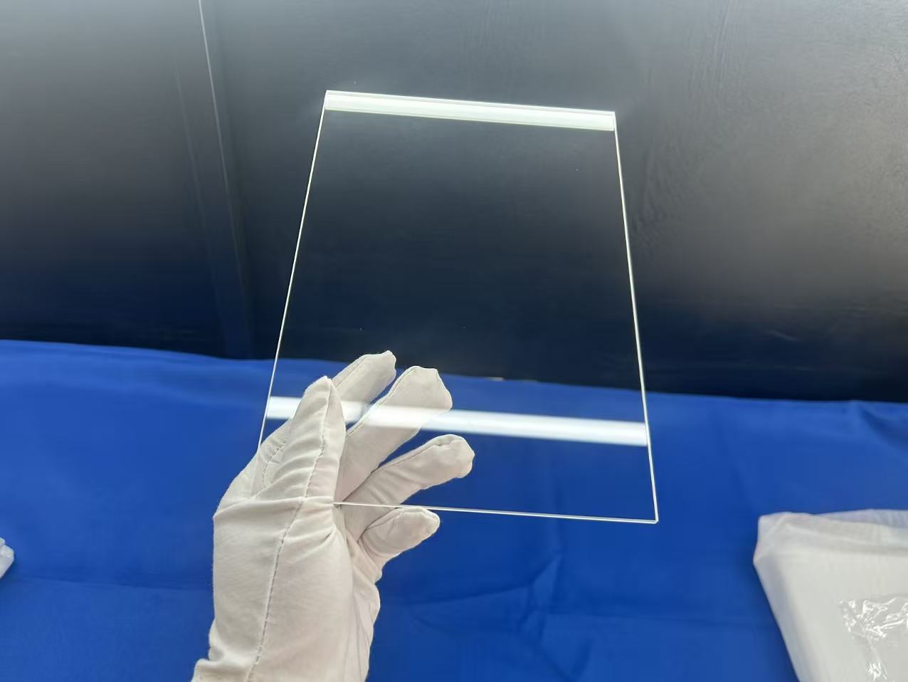
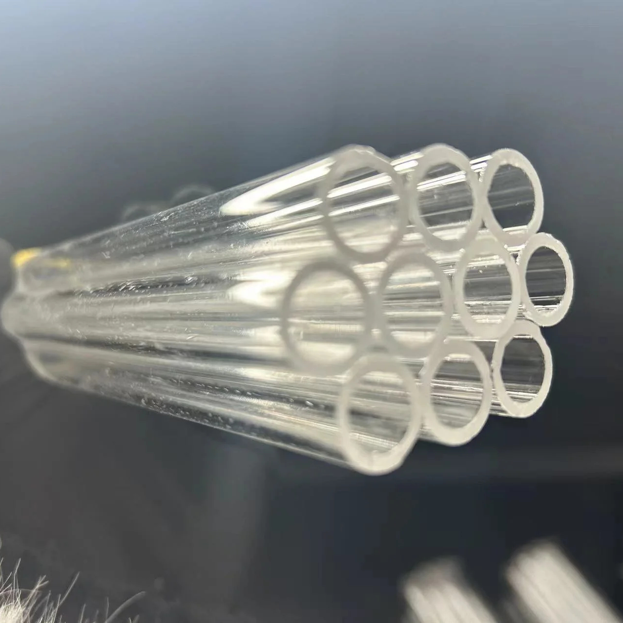
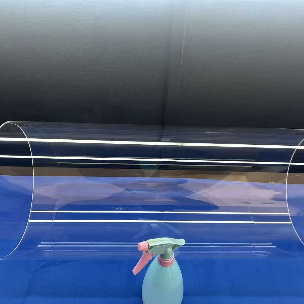
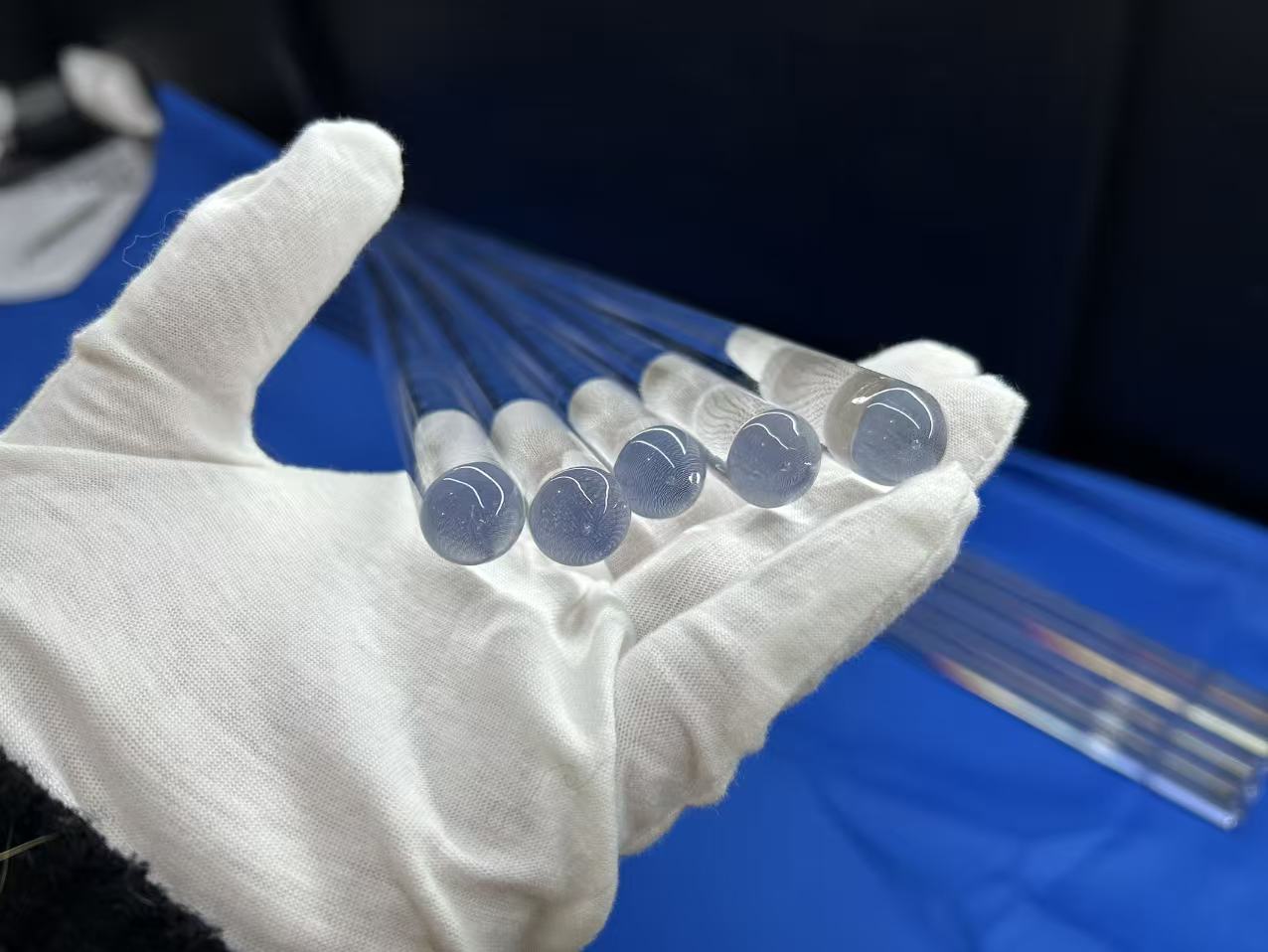
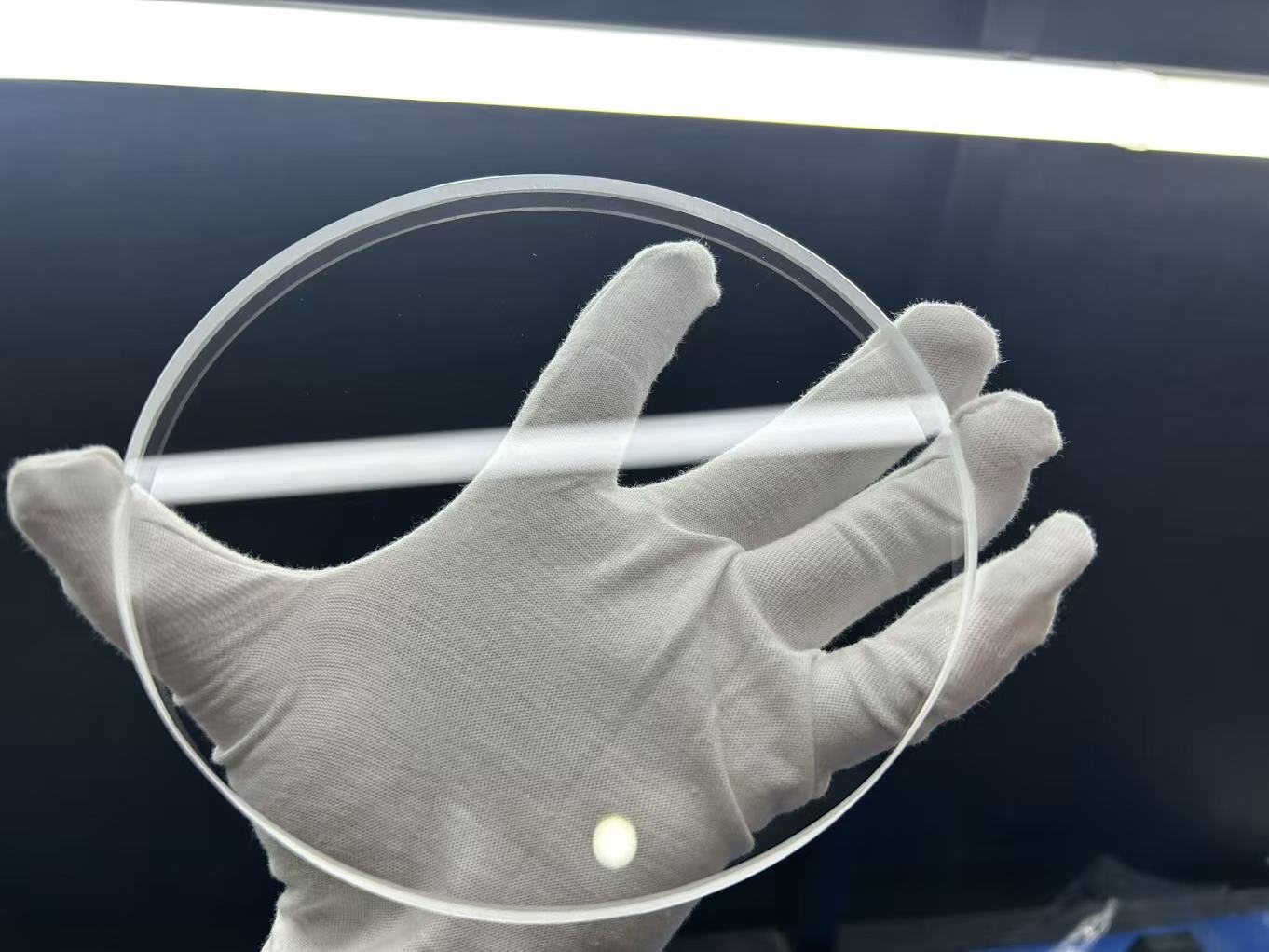
Physical Crystallography & Optical Substrate Metallurgy
Comprehensive technical guidance for optoelectronic design engineers, materials scientists, and procurement executives across Wrocław and the Lower Silesian high-tech cluster.
Crystallographic Orientations of Monocrystalline Corundum (Al₂O₃)
Synthetic monocrystalline sapphire (α-Al₂O₃, hexagonal rhombohedral structure) is an indispensable material for extreme photonic, semiconductor, and aerospace applications. Unlike isotropic fused quartz or amorphous optical glasses, single-crystal sapphire exhibits distinct anisotropic mechanical, thermal, and optical properties dictated by its crystallographic orientation. Selecting the appropriate orientation is paramount for engineers designing epitaxial substrates, laser cavity viewports, or cryogenic RF windows.
C-Plane (0001) Substrates
The standard orientation for III-V nitride heterostructures (GaN, InGaN, AlGaN). Its hexagonal symmetry matches lattice spacing for high-brightness blue/UV LEDs, laser diodes, and high-electron-mobility transistors (HEMTs). Zero birefringence occurs perpendicular to the optic axis.
R-Plane (1-102) Substrates
Oriented at 57.6° to the C-plane, R-plane substrates exhibit a pseudo-cubic structure. Primarily utilized in Silicon-on-Sapphire (SOS) CMOS devices, ultra-radiation-hardened space microelectronics, and non-polar GaN growth to eliminate quantum-confined Stark effects.
A-Plane (11-20) Substrates
Uniformly non-polar orientation with a 90° relationship to the optic axis. Ideal for high-density magnetic storage media, optical isolators, polarized optical waveplates, and hybrid optocouplers requiring a stable dielectric environment up to 10 GHz.
M-Plane (10-10) Substrates
Non-polar orientation situated perpendicular to the c-axis planes. M-plane wafers prevent internal piezoelectric polarization fields, yielding dramatically higher radiative recombination efficiency in green laser diodes and vertical-cavity surface-emitting lasers (VCSELs).
Sapphire vs. High-Purity Fused Quartz: Comprehensive Property Matrix
In high-power industrial photonics and vacuum semiconductor processing in Lower Silesia, selecting between sapphire substrates and fused silica (JGS1, JGS2, JGS3) depends on thermal gradients, optical transmission spectrum, and mechanical erosion factors.
| Physical / Engineering Property | Monocrystalline Sapphire (Al₂O₃) | Synthetic Fused Silica (JGS1) | Optical Fused Quartz (JGS2) | IR-Grade Quartz (JGS3) |
|---|---|---|---|---|
| Chemical Formula & Structure | Single Crystal α-Al₂O₃ (Trigonal) | Amorphous High-Purity SiO₂ | Amorphous Natural Quartz SiO₂ | Low-OH Fused Quartz SiO₂ |
| Optical Transmission Range | 0.19 – 5.5 µm (Deep UV to Mid-IR) | 0.185 – 2.5 µm (Deep UV) | 0.220 – 2.5 µm (UV-Vis) | 0.260 – 3.5 µm (Vis to Mid-IR) |
| Mohs Hardness / Knoop | Mohs 9 (1800–2200 kg/mm²) | Mohs 5.5–6.5 (460 kg/mm²) | Mohs 5.5–6.5 (460 kg/mm²) | Mohs 5.5–6.5 (460 kg/mm²) |
| Thermal Conductivity (20°C) | 40 W/(m·K) (Parallel to C) | 1.38 W/(m·K) | 1.38 W/(m·K) | 1.38 W/(m·K) |
| Coefficient of Thermal Expansion | 5.8 × 10⁻⁶ /K (Parallel to C) | 5.5 × 10⁻⁷ /K (Zero-warp) | 5.5 × 10⁻⁷ /K | 5.5 × 10⁻⁷ /K |
| Max Working Temperature | 2000°C (Short-term) / 1600°C (Cont.) | 1450°C (Short) / 1100°C (Cont.) | 1400°C (Short) / 1050°C (Cont.) | 1400°C (Short) / 1050°C (Cont.) |
| Chemical Resistance | Inert to all acids, HF < 300°C | Resistant to acids, attacked by HF | Resistant to acids, attacked by HF | Resistant to acids, attacked by HF |
High-Tech Photonics & Industrial Integration in Wrocław
Wrocław has established itself as Central Europe’s Silicon Enclave. From academic microelectronics incubators to heavy industrial laser fabrication, our components drive critical regional applications.
The Wrocław Technology & R&D Hub
Home to the prestigious Wrocław University of Science and Technology (Politechnika Wrocławska), Łukasiewicz Research Network – PORT Polish Center for Technology Development, and the Wrocław Technology Park (WPT), the city is a vanguard of photonics, quantum computing, and wide-bandgap semiconductor commercialization.
Our manufacturing supply chain provides direct, tariff-compliant OEM integration of epi-ready sapphire substrates, laser optical cavities, and custom fused quartz furnace tubes to laboratories and high-volume factories across Dolnośląskie.

1. High-Power Fiber Laser Optics & Nozzle Windows
Lower Silesia boasts Poland's highest density of metal processing, automotive tier-1 manufacturing, and industrial automation. Multi-kilowatt (10 kW–30 kW) laser cutting and CNC welding heads require optical sapphire protective windows due to sapphire’s extreme thermal shock thresholds, low absorption coefficient at 1064–1070 nm, and imperviousness to molten metallic spatter.
2. GaN / InGaN Epi-Ready Substrates for Power Electronics
R&D consortia around Łukasiewicz – PORT and regional fabless chip design houses are pioneering GaN-on-sapphire architectures. Nivra Quartz supplies double-sided polished (DSP) C-plane wafers with atomic step terrace morphology, total thickness variation (TTV) < 1 µm, and surface roughness Ra < 0.2 nm, providing flawless lattice templates for next-gen EV power converters and fast-charging modules.
3. Cryogenic & Vacuum Viewports in Analytical Physics
Academic institutes in Wrocław specializing in solid-state physics, Raman spectroscopy, and ultracold quantum systems utilize our sapphire-to-kovar brazed viewport assemblies and high-purity JGS1 fused quartz bell jars. Sapphire maintains crystal lattice integrity and optical clarity even at liquid helium temperatures (4.2 K) under ultra-high vacuum (< 10−10 mbar).
Wrocław Photonics & Semiconductor Procurement Dynamics
Analyzing key structural shifts in Lower Silesian advanced material procurement, clean energy transitions, and resilient B2B global supply integration.
Supply Chain Decoupling & Direct Foundry Engagement
European optoelectronics firms historically purchased through third-party intermediaries in Western Europe, adding 35%–55% distributor markups and 8-week delays. Wrocław OEMs now bypass intermediary layers, working directly with established China-based foundries like Nivra Quartz to secure AS9100/ISO-certified sapphire ingots, precision dicing, and fast air courier deliveries straight to Copernicus Airport Wrocław (WRO).
Accelerating European Microelectronics & EU Chips Act Inflows
Significant investments along the Wrocław-Katowice corridor under the European Chips Act are driving domestic packaging, assembly, and test (OSAT) infrastructure. As multi-million-euro fab facilities ramp up cleanroom operations in Dolnośląskie, demand for custom sapphire carrier discs, wafer bonding substrates, and chemical-mechanical planarization (CMP) quartz consumables has surged by over 42% year-on-year.
Stringent Cleanliness & Defect Metrology Standards
R&D groups in Lower Silesia no longer accept generic industrial-grade crystals. Sourcing contracts strictly mandate sub-angstrom surface roughness, laser interferometer verification of wavefront distortion (λ/10 @ 632.8 nm), class 100 cleanroom vacuum packaging, and certified lot traceability from Kyropoulos boule seed to finished wafer.
Why Tier-1 Engineers & Procurement Teams Partner with Nivra Quartz
Combining Donghai County’s premier crystal capital raw material base with advanced Swiss/German grinding, polishing, and cleanroom metrology machinery.
End-to-End In-House Processing
From single-crystal growth (Kyropoulos & HEM methods) to multi-axis diamond wire sawing, double-sided CMP planarization, ultrasonic cleaning, and optical thin-film anti-reflective (AR) coating. Complete ownership guarantees consistent quality and competitive pricing.
Cleanroom Inspection & Metrology
Every wafer and optical component undergoes Zygo optical surface interferometry, atomic force microscopy (AFM), and polarized stress analysis inside an ISO Class 5 / Class 100 cleanroom environment prior to vacuum packaging in sealed Fluoroware cassettes.
Rapid Technical Feedback ≤ 5h
Our bilingual optical engineering team reviews custom drawings (STEP, DWG, PDF) within 5 working hours, offering DFM (Design for Manufacturability) advice, tolerance optimization, and rapid air prototyping directly into Wrocław within 4–6 business days.
EU Customs & DAP Logistics
Extensive experience with Polish customs clearance, EORI registered shipments, HS code categorization (avoiding unwarranted import tariff disputes), and specialized shock-proof vacuum crate packaging to protect fragile optics against handling vibration.
Frequently Asked Questions for Sourcing in Wrocław, Poland
Essential commercial, technical, and logistics clarifications addressing common queries from engineering buyers and university research labs across Lower Silesia.
Request an Engineering Consultation & Quotation
Send your dimensional drawings, CAD files (STEP / DWG / PDF), material specifications, and tolerance requirements. Our application engineering team will review manufacturability and provide an official quotation within 5 hours.