High-Purity Quartz & Optical Components for Silicon Valley OEMs
Direct from our Donghai manufacturing hub to Santa Clara R&D laboratories and cleanroom production lines. Fully certified optical substrates, thermal vessels, and precision glassware.
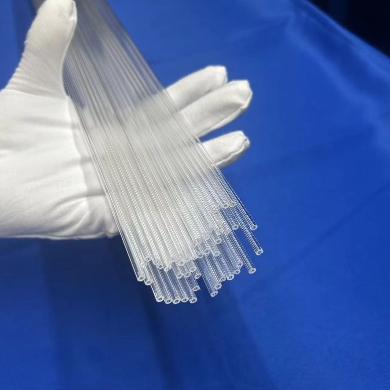
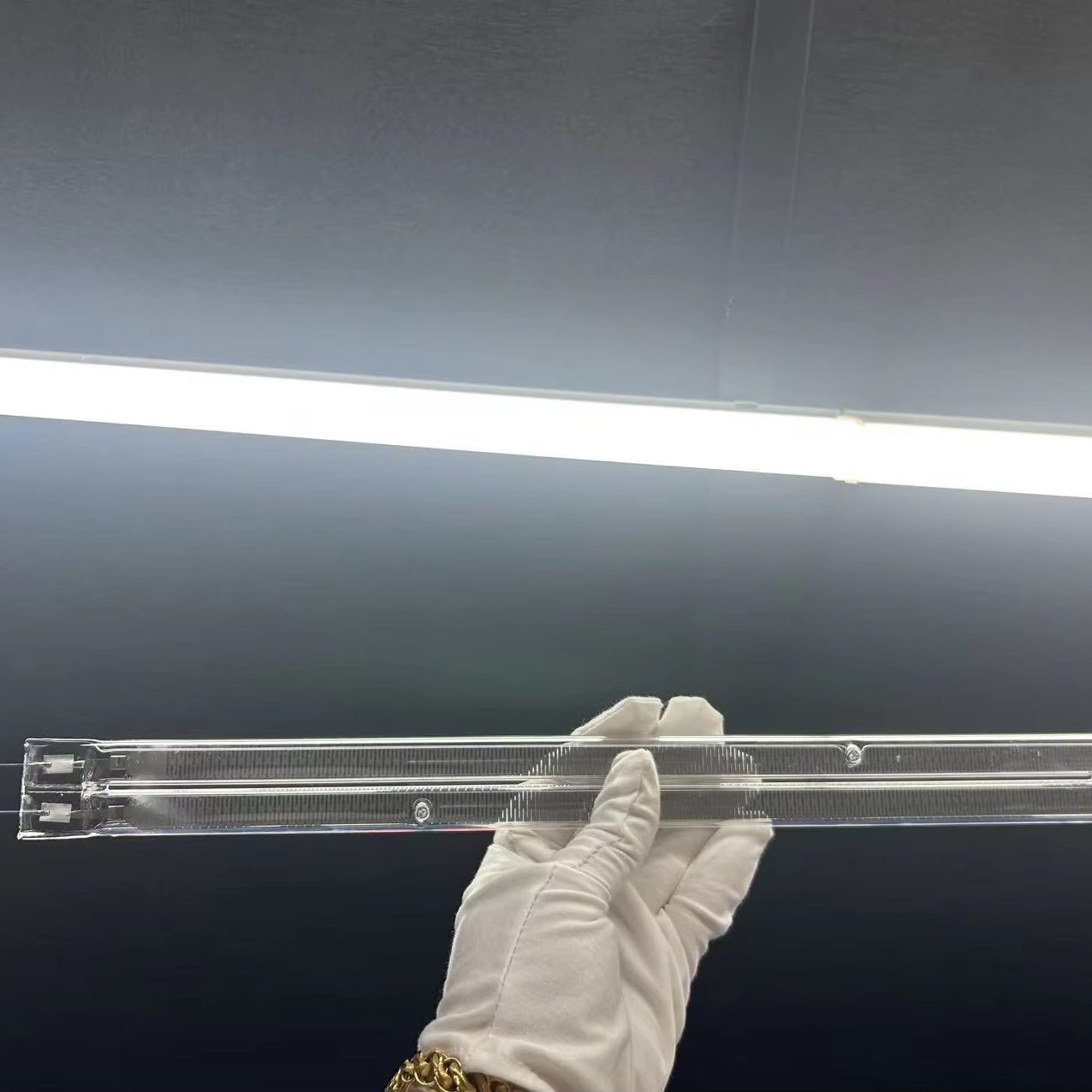
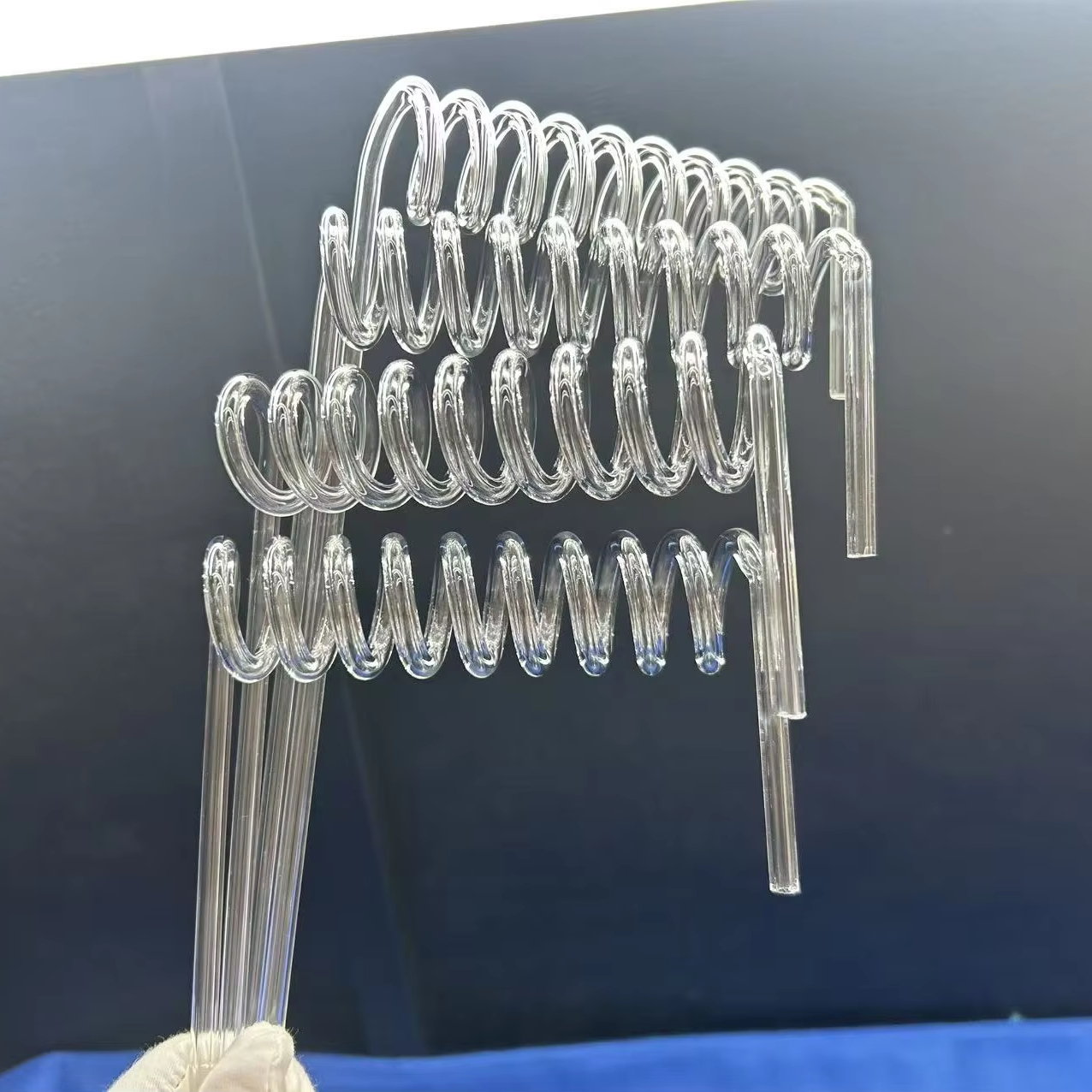
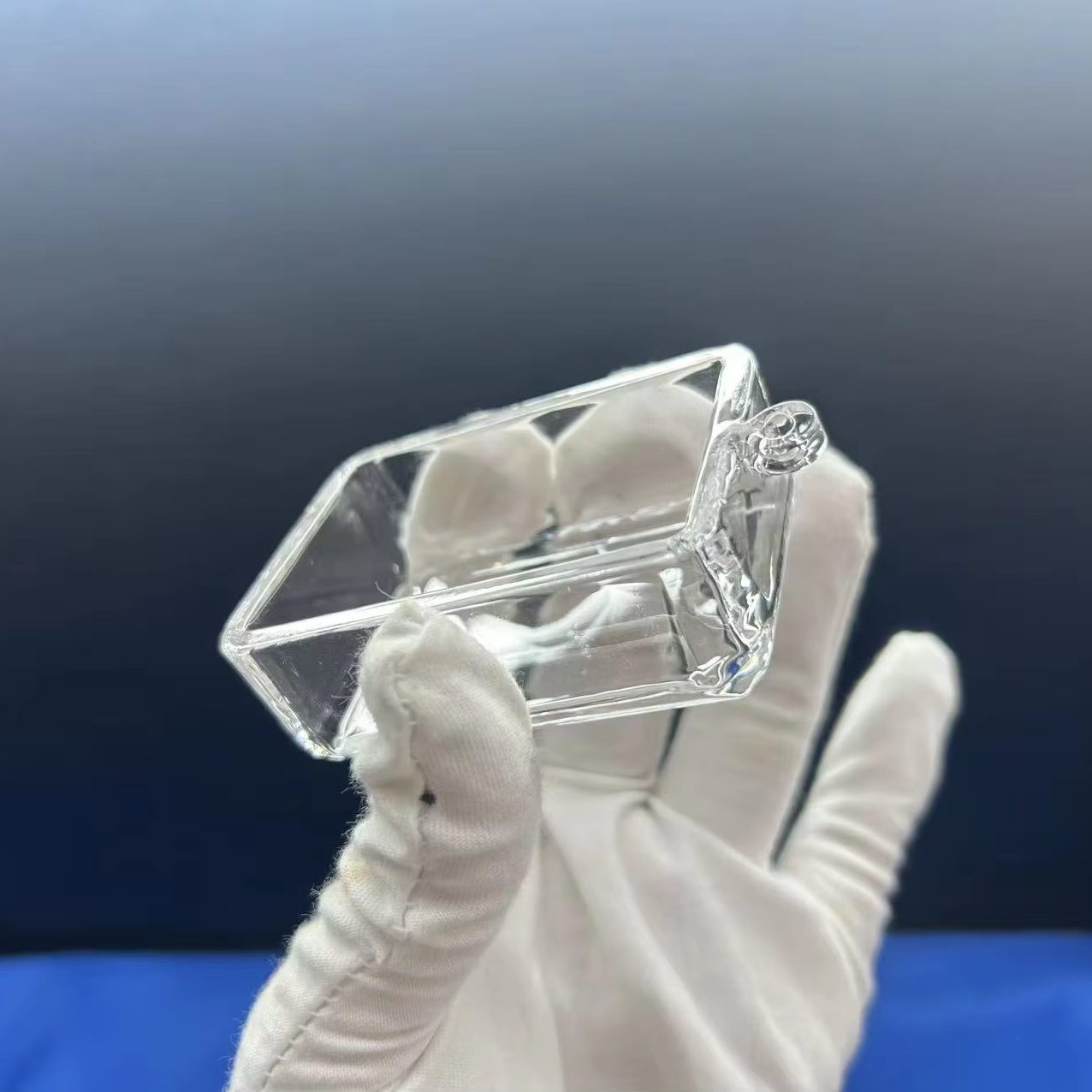
Engineering Optical Quartz Prisms for Silicon Valley's Next-Generation Photonic Architectures
The Santa Clara technology corridor—spanning the heart of Silicon Valley from Expressway cleanrooms to autonomous driving testing grounds—commands the most stringent optical tolerances in global engineering. Whether routing high-energy ultraviolet laser pulses in semiconductor wafer defect inspection systems, folding multi-axis light paths inside AI datacenter optical transceivers, or maintaining phase synchronization in quantum computing cryostats, optical quartz prisms are mission-critical components that dictate the ultimate signal-to-noise ratio and reliability of the end device.
At Donghai County Nivra Quartz Products Co., Ltd., we bridge the gap between raw natural and synthetic quartz crystalline purity and extreme nanoscale optical fabrication. By maintaining a complete vertically integrated processing facility with over 100 experienced technicians, state-of-the-art CNC grinding centers, double-sided planetary pitch polishers, and Zygo laser interferometric measurement, we supply Santa Clara procurement engineers with precision-engineered optical quartz prisms that eliminate optical dispersion errors, withstand high thermal stresses, and guarantee sub-arcsecond angular tolerances.
1. Substrate Grade Selection: JGS1 Synthetic Silica vs. JGS2 Optical Quartz vs. JGS3 Low-OH
Understanding substrate thermodynamics and spectral transmission profiles is crucial when drafting optical fabrication prints for Bay Area hardware incubators:
| Substrate Grade | Material Synthesis & Structure | Transmission Bandwidth | Hydroxyl (OH⁻) Content | Primary Santa Clara Application |
|---|---|---|---|---|
| JGS1 (Synthetic Fused Silica) | Synthetic chemical vapor deposition (SiCl₄ flame hydrolysis), zero crystalline inclusions, bubble class 0. | 185 nm – 2500 nm (Deep UV optimized) | < 1200 ppm (Typical) | Semiconductor EUV/DUV steppers, wafer inspection laser optics, excimer laser line beam splitters. |
| JGS2 (Optical Grade Fused Quartz) | Electric vacuum fusion of high-purity natural quartz crystals from select Donghai geological deposits. | 220 nm – 2500 nm (UV-Visible standard) | < 30 ppm | Spectroscopy dispersion prisms, analytical sensor flow-cells, precision reference optical flats. |
| JGS3 (Infrared Synthetic Silica) | Gas-refined electric fusion with severe water-desorption degassing; devoid of absorption dip at 2730 nm. | 260 nm – 3500 nm (Wide IR transparency) | < 5 ppm (Ultra-dry) | Thermal imaging folding prisms, high-power Nd:YAG and fiber laser optics (1064nm – 2100nm). |
2. Geometry Variants & Beam-Manipulation Physics
Santa Clara photonics teams leverage our precision prisms across diverse geometries, each fabricated with exact beveling and scratch-dig controls:
- Right-Angle Prisms (RAP): Utilized for 90° beam deflection via Total Internal Reflection (TIR) or external hypotenuse reflection. When coated with high-damage-threshold dielectric anti-reflection (AR) films on entry/exit faces, transmission exceeds 99.5% at target laser lines.
- Penta Prisms & Dove Prisms: The penta configuration provides precise 90° beam deviation without sensitivity to mechanical tilt or vibration—making it essential for Santa Clara automated wafer handling arms and robotic optical alignment rigs. Dove prisms provide image rotation at twice the angular velocity of the prism rotation.
- Corner Cube Retroreflectors: Fabricated with three mutually perpendicular reflecting surfaces. Light entering the retroreflector is returned parallel to its incident path regardless of the prism's spatial orientation, which is crucial for autonomous vehicle LiDAR calibration along Silicon Valley transit arteries.
- Equilateral & Brewster Dispersion Prisms: Precise apex angle machining separates broadband optical spectrums into distinct spatial wavelengths with minimal polarization-induced Fresnel losses.
High-Tech Santa Clara Applications for Precision Quartz Prisms
Santa Clara's technology ecosystem requires optical components capable of functioning flawlessly under extreme thermal loads, chemical exposure, and sub-nanometer alignment requirements.
Semiconductor Metrology & EUV Mask Inspection
Fabricated in ultra-pure JGS1 synthetic silica, our prisms steer 193nm and 266nm inspection beams across patterned silicon wafers. Negligible fluorescence and minimal solarization resist photochemical degradation in 24/7 fab operations.
AI Co-Packaged Optics & Optical Interconnects
Hyperscale datacenter accelerators developing 800G and 1.6T transceivers utilize micro-prisms for coupling multi-fiber arrays into silicon photonic PICs, delivering sub-micron spatial positioning and insertion losses under 0.2 dB.
LiDAR & Autonomous Vehicle Sensor Suites
Automotive tech teams based along the San Tomas Expressway integrate customized fused silica roof-mount retroreflectors and beam splitters that maintain angular accuracy from -40°C to +125°C without thermal drift.
Medical Instrumentation & Flow Cytometry
South Bay life-science instrumentation manufacturers use quartz flow prisms and spectroscopic cuvettes to analyze blood markers. Quartz's optical purity eliminates background autofluorescence across UV-visible ranges.
Ultrafast Laser Pulse Compression (Femtosecond Labs)
High-damage-threshold fused silica prism pairs manage Group Delay Dispersion (GDD) in femtosecond titanium:sapphire and fiber laser amplifiers deployed in university and industrial labs across Stanford and Santa Clara.
Aerospace Navigation & Ring Laser Gyroscopes
Defense contractors and aerospace avionics builders in Silicon Valley incorporate our ultra-low expansion, zero-birefringence total reflection quartz prisms into inertial navigation guidance systems.
Silicon Valley Sourcing Dynamics: Why Santa Clara Engineering Teams Dual-Source with Nivra Quartz
The procurement landscape across Santa Clara, Sunnyvale, and San Jose is experiencing a profound transition. In the past, hardware developers relied exclusively on regional domestic distributors who marked up optical parts by 300% to 500% while imposing 16-to-24-week lead times. Today, rapid hardware iteration in high-compute AI photonics and advanced packaging demands agility, transparency, and direct manufacturing partnerships.
By establishing a direct procurement bridge with Nivra Quartz in Donghai County—the global nucleus of quartz raw materials and optical processing—Bay Area organizations gain three decisive strategic benefits:
Compressed Sprint Cycles
Rapid CNC pre-forming and dedicated prototype cells turn custom optical prism drawings into physical evaluation samples in as little as 10 to 14 days, supported by express air freight directly to San Francisco (SFO) or San Jose (SJC) international hubs.
Bespoke Sub-Arcsecond Metrology
Every prism export destined for the Santa Clara tech sector includes NIST-traceable Zygo interferograms, spectrophotometric transmission curves, and surface roughness atomic force microscopy (AFM) documentation to expedite incoming dock-to-stock QC clearance.
Direct Factory Economics
Eliminating multiple tiers of brokers and domestic repackagers allows Silicon Valley teams to reallocate capital toward R&D scaling, enjoying Tier-1 raw material purity (SiO₂ ≥ 99.99%) at genuine factory-direct volume pricing.
Precision Specifications & Fabrication Limits
Refer to our standard engineering tolerances and physical benchmarks when designing optical quartz assemblies.
| Dimensional / Optical Metric | Commercial Grade | Precision Lab Grade | High-Precision Fab Spec (OEM Custom) |
|---|---|---|---|
| Dimension Tolerance | ±0.10 mm | ±0.05 mm | ±0.010 mm (±10 μm) |
| Angular Accuracy | ±3 arcmin (≤ 180") | ±30 arcsec (≤ 30") | ±1 to 3 arcsec (≤ 3") |
| Surface Flatness (P-V @ 632.8 nm) | λ / 2 | λ / 4 | λ / 10 to λ / 20 |
| Surface Quality (MIL-PRF-13830B) | 60 / 40 | 40 / 20 | 10 / 5 (Ultra-low scatter laser grade) |
| Clear Aperture | > 85% Central Area | > 90% Central Area | > 95% Central Area |
| Chamfer / Bevel | 0.2 – 0.5 mm × 45° | 0.1 – 0.3 mm × 45° | Protective micro-chamfer <0.05 mm |
| Laser Damage Threshold (LIDT) | > 5 J/cm² (1064nm, 10ns) | > 10 J/cm² (1064nm, 10ns) | > 18 J/cm² (1064nm, 20Hz, 10ns pulsed) |
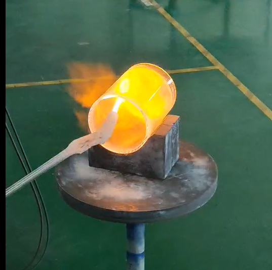
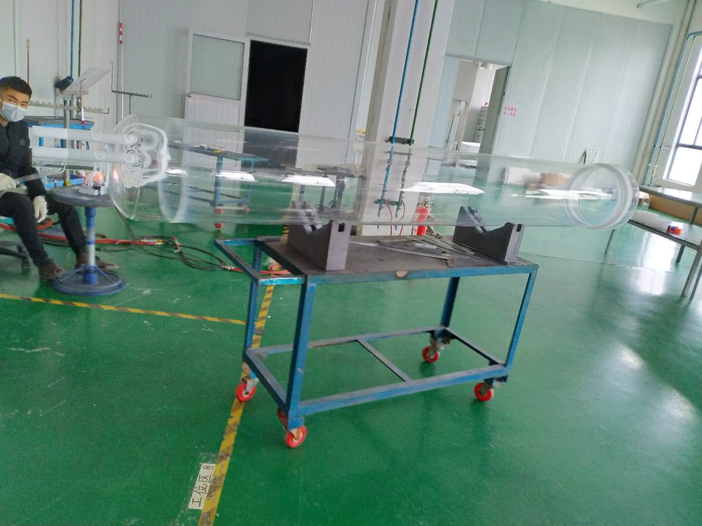
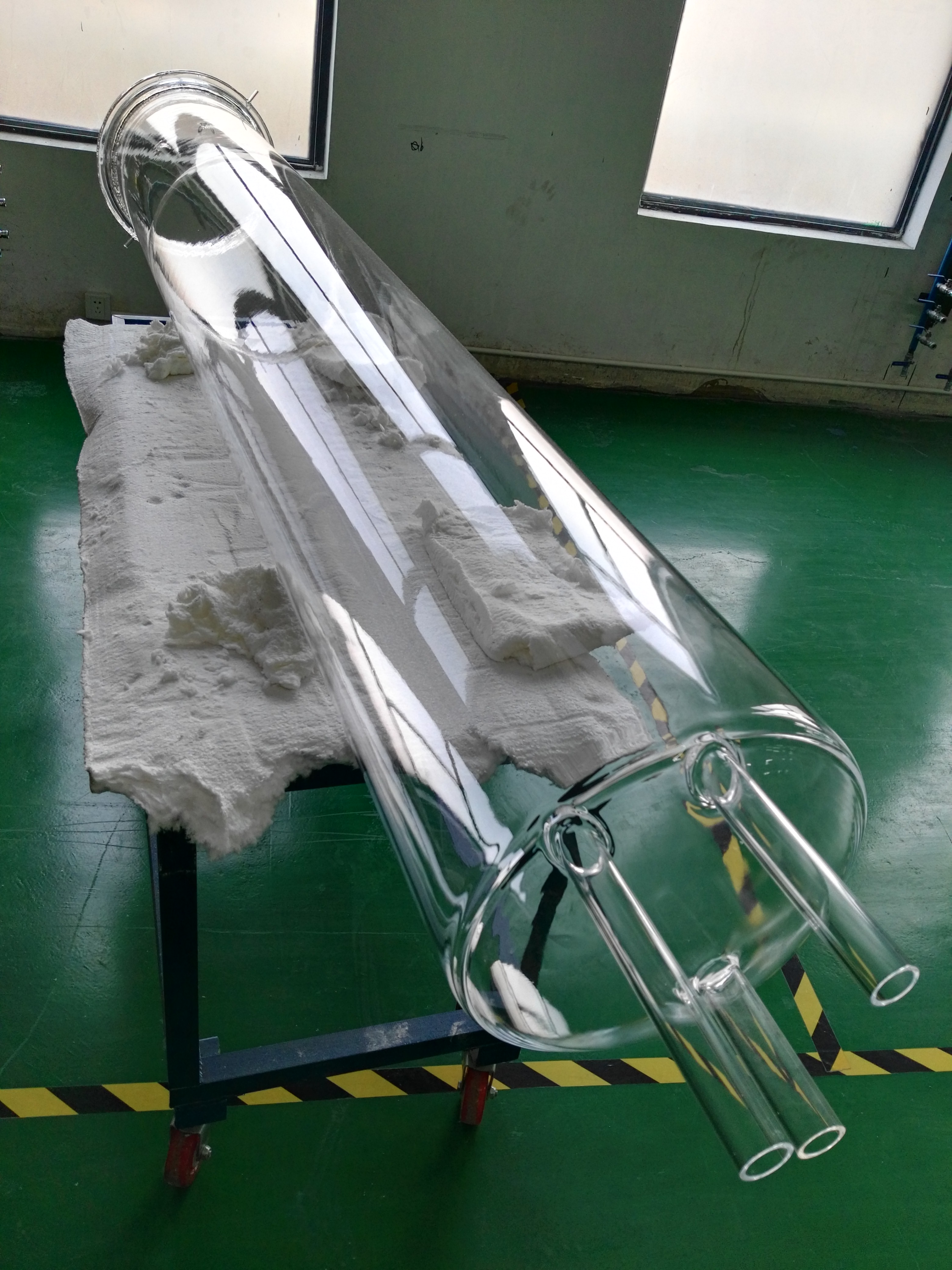
In-House Manufacturing & Optical Metrology at Nivra Quartz
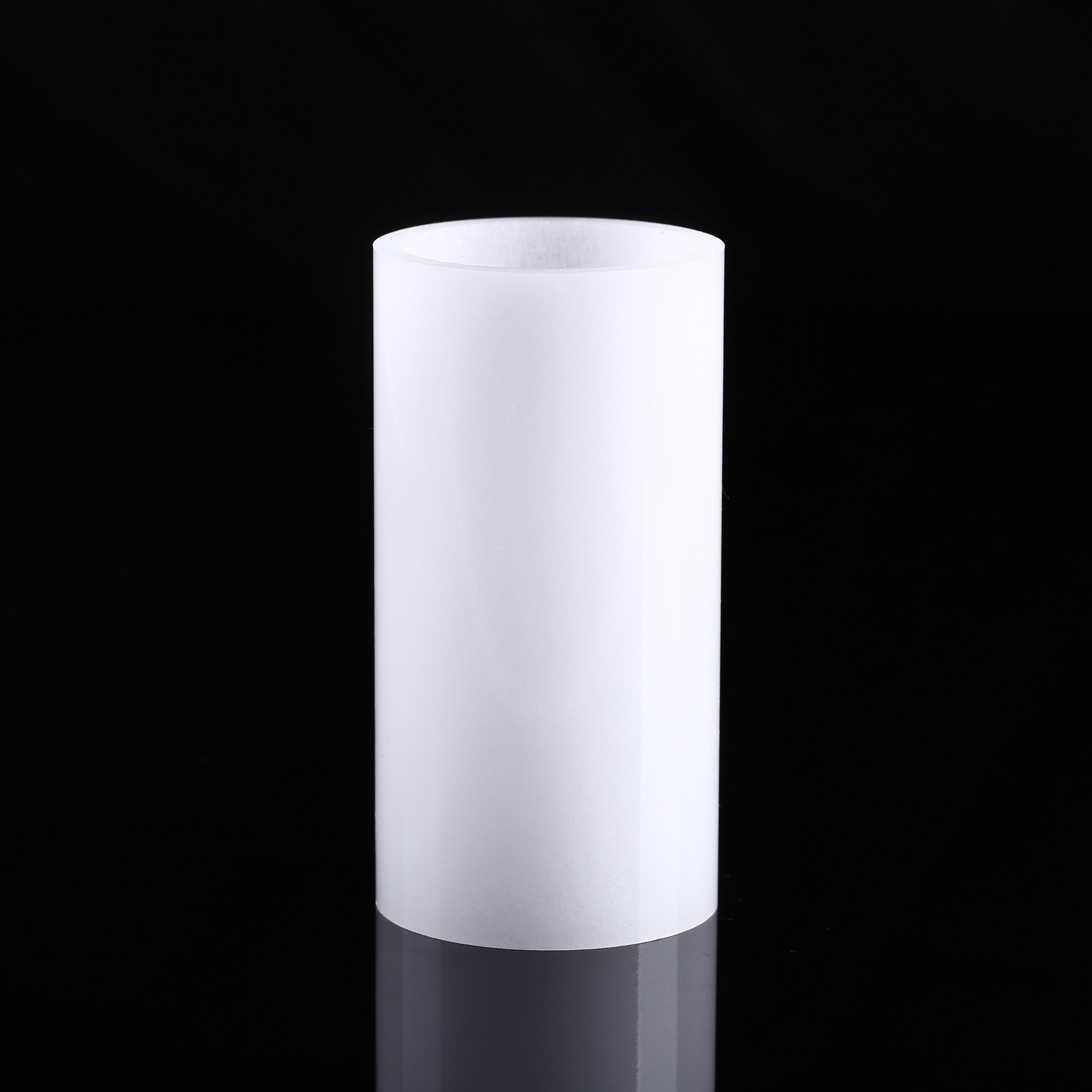
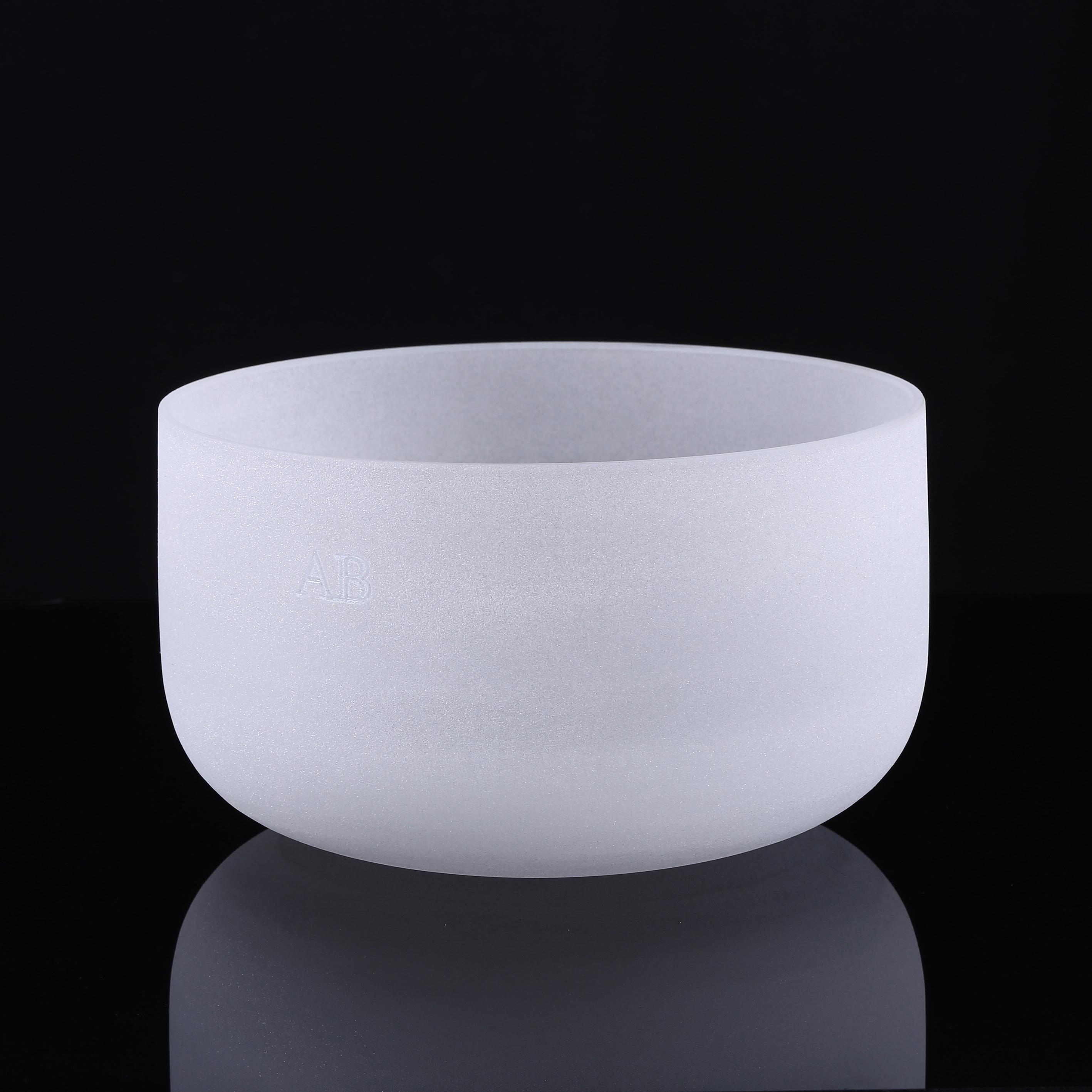
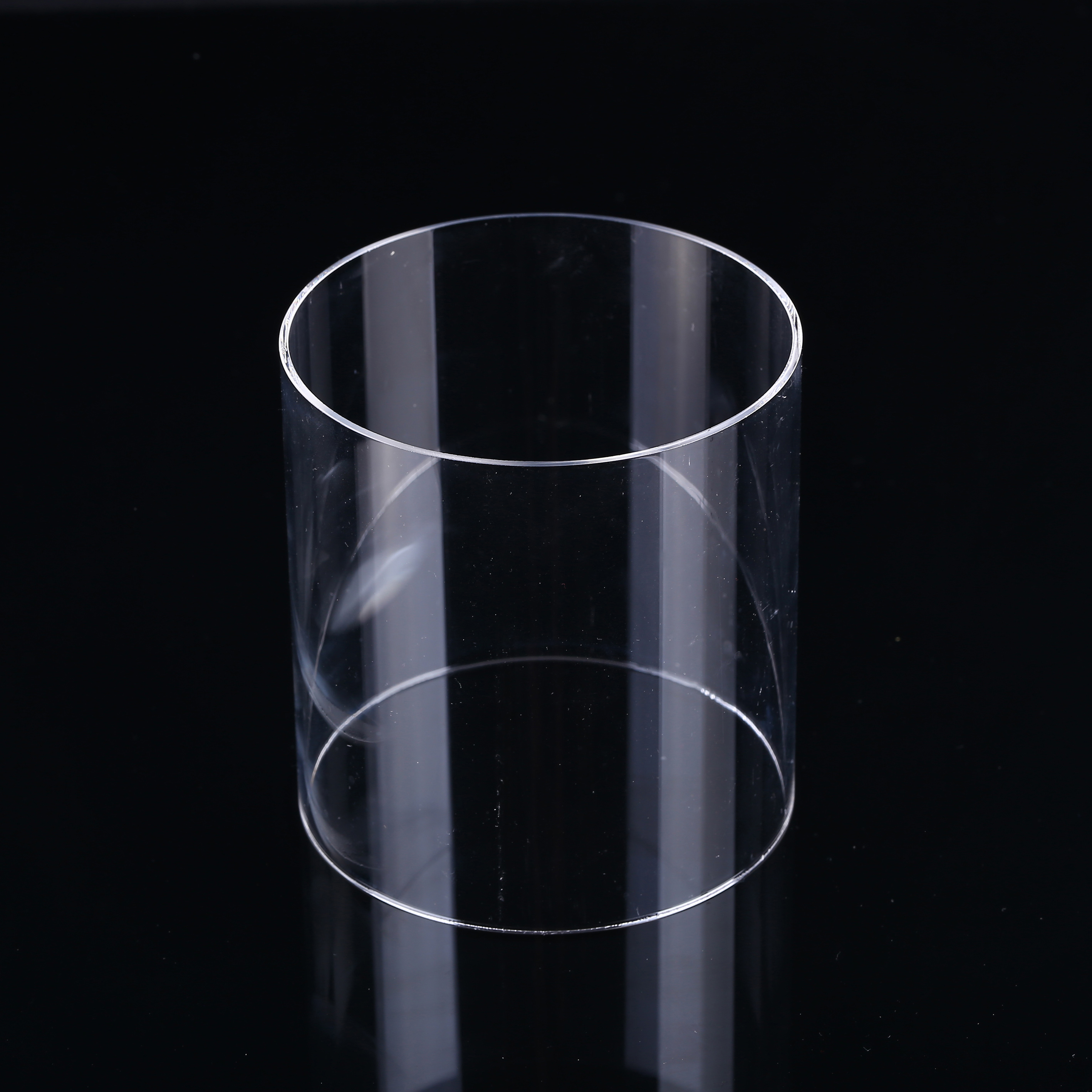
Manufacturer Credibility, Scale & Verification
Donghai County Nivra Quartz Products Co., Ltd. has operated in the quartz capital of China since 2019, combining localized mineral access with modern quality controls.
Integrated Ecosystem
Located at 285 Heping East Road, Lianyungang, Jiangsu, our access to ultra-pure crystalline quartz reserves keeps raw material overhead low without purity compromise.
101–200 Skilled Specialists
A seasoned workforce of flame masters, optical polishers, and optical metrology technicians ensuring zero-defect batch runs for every export consignment.
≤5-Hour Engineering Turnaround
Our sales engineering desk operates across Pacific Standard Time (PST) overlaps. We achieve an 88.89% inquiry response rate with comprehensive DFM design feedback.
Verified Export Integrity
On-site verified facilities by Alibaba.com and third-party inspectors, maintaining a 5.0/5 customer service and product quality track record across North America.
Verified corporate licenses and ISO certification credentials available upon request for Santa Clara vendor onboarding:
Frequently Asked Questions by Santa Clara Optical Engineers
Practical guidance on material grades, logistics, customs clearance, optical coatings, and custom manufacturing workflows.
Accelerate Your Santa Clara Photonics Project Today
Send our senior engineering team your prism prints, tolerance specifications, or laser system parameters. We provide DFM optimization, detailed pricing, and metrology roadmaps within 5 business hours.