High-Purity Quartz Product Portfolio
Factory-direct OEM/ODM quartz components precision-engineered for wafer fabrication, chemical synthesis, and thermal processing in Osaka industrial zones.
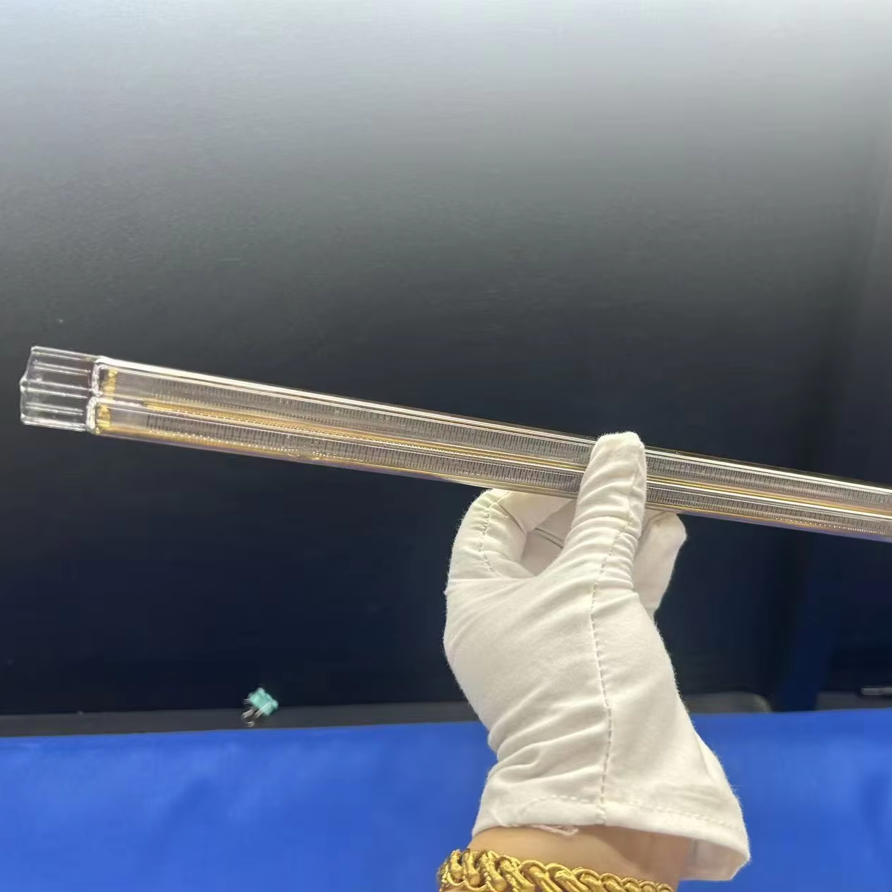
Graphene Quartz Heating Tube
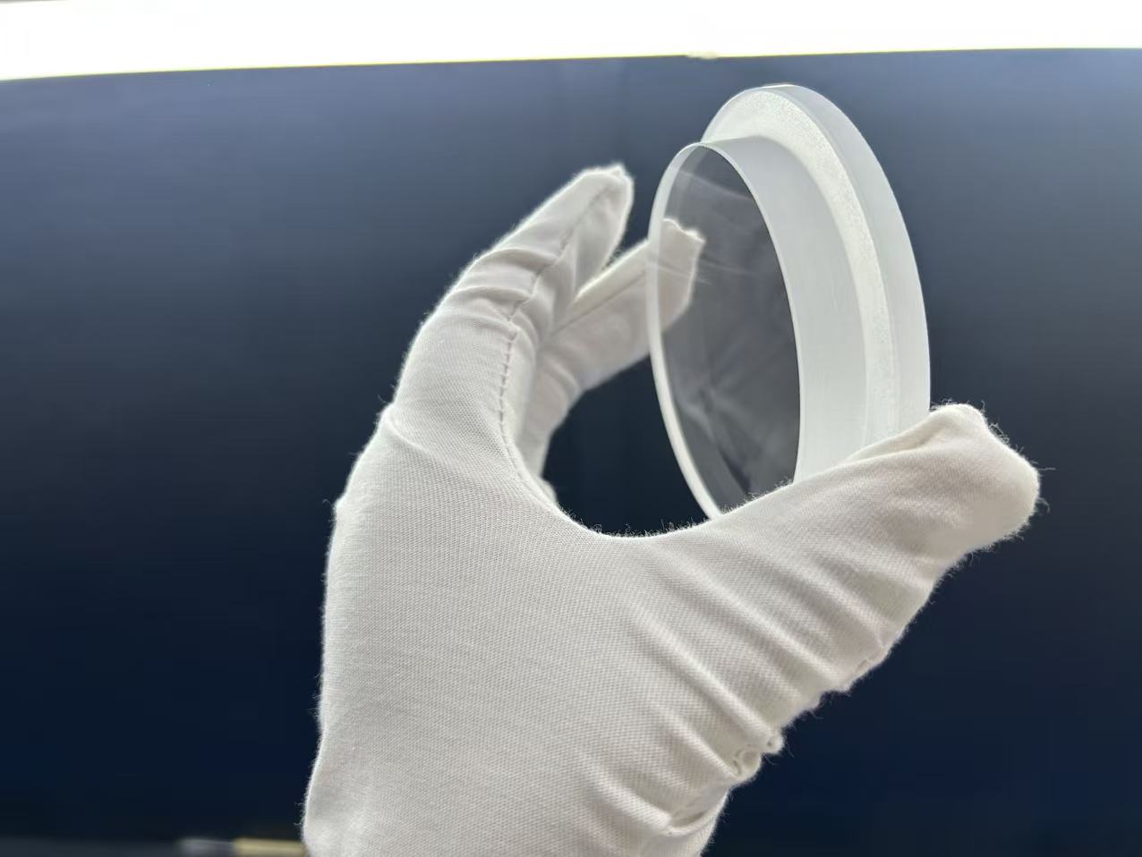
Factory-Made High-Purity Ultra-Thick Quartz Step Plate
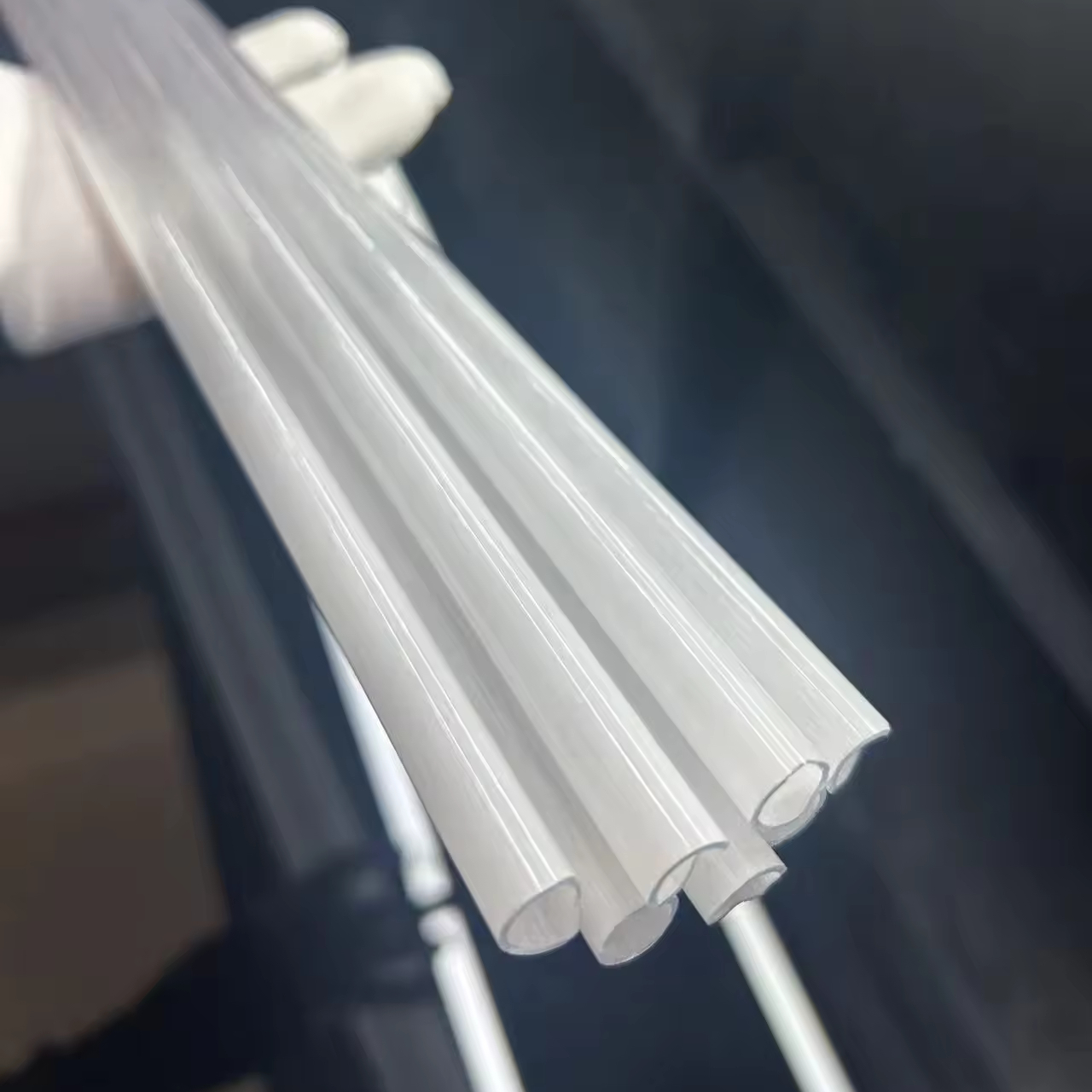
Translucent & Opaque Milky White Quartz Glass Tube
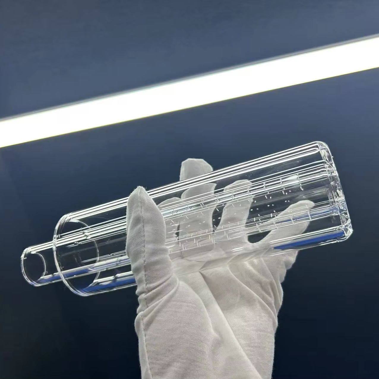
Customized Perforated Quartz Tube
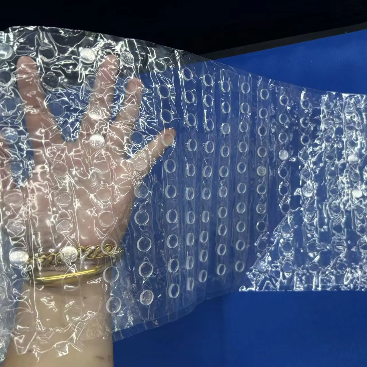
Factory-Made High-Purity Small Size Quartz Wafer
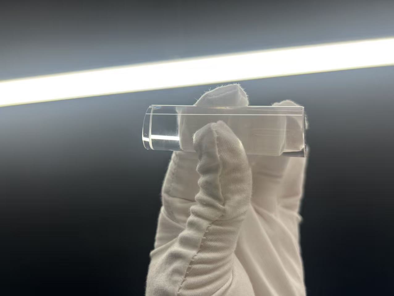
Round Head Precision Quartz Rod
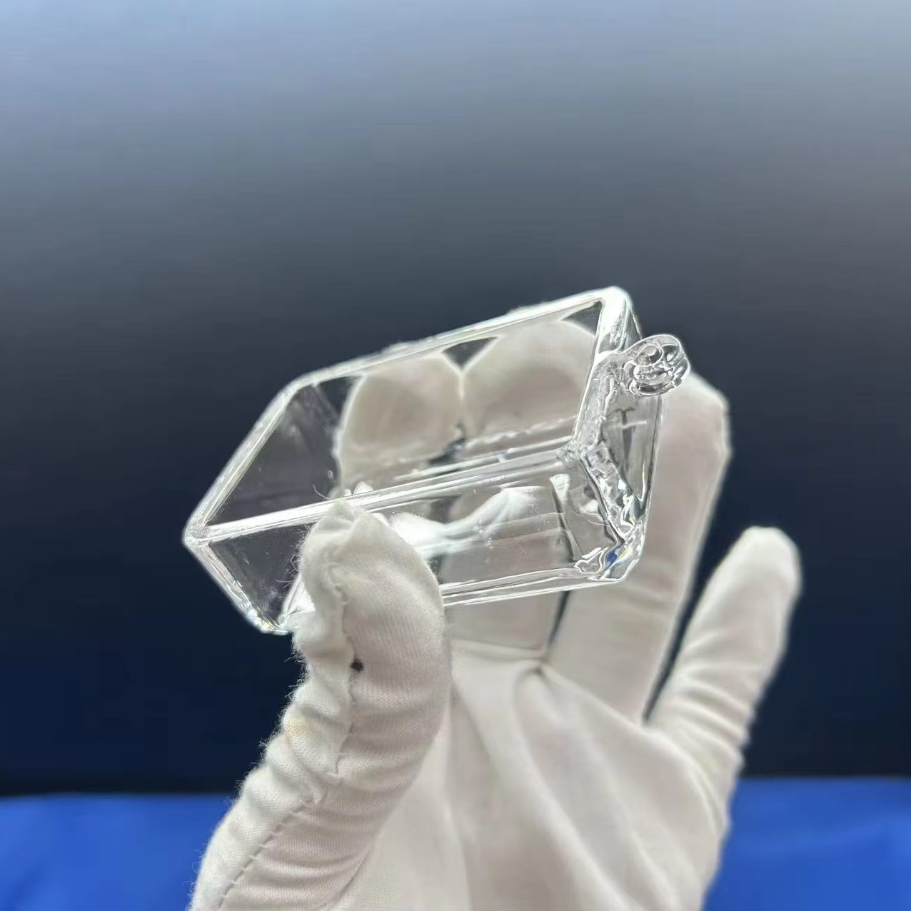
High-Purity Welded Quartz Tank
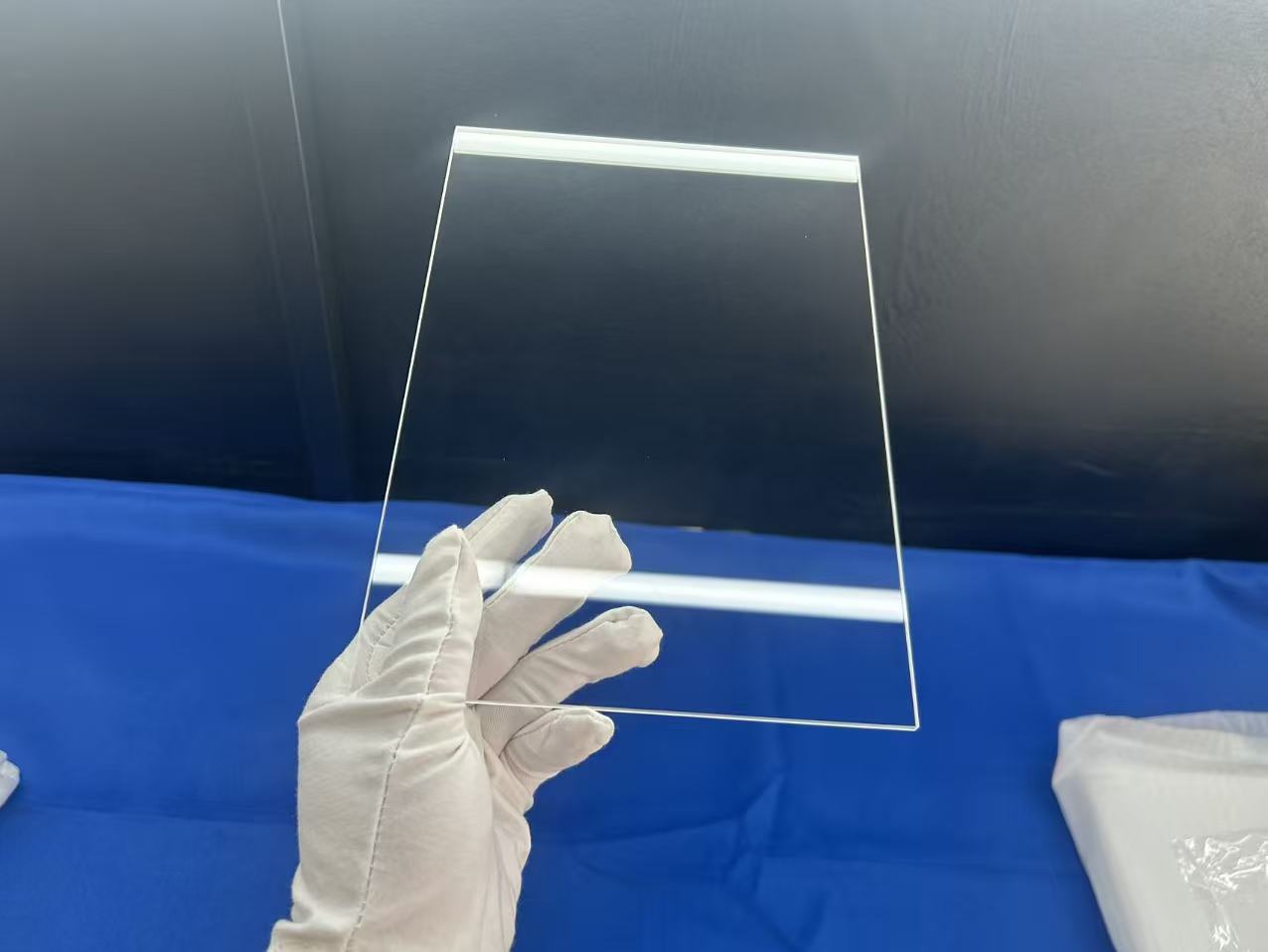
Custom Polished Square Quartz Glass Plate (3mm)
Executive Technical Report: The Strategic Role of Quartz Wafers in Kansai's High-Tech Supply Chain
Osaka and the greater Kansai region represent the technological backbone of Japan’s advanced electronics, semiconductor fabrication equipment, and green energy technology sectors. As semiconductor geometries shrink below 3nm and photovoltaic cells transition toward ultra-high efficiency TOPCon and Heterojunction (HJT) architectures, the purity and structural integrity of process substrates have become paramount. High-purity fused quartz wafers, synthesized silica plates, and custom quartz glass vessels are essential elements in eliminating trace metal contamination during high-temperature thermal oxidation, diffusion, etching, and chemical vapor deposition (CVD).
As a specialized OEM/ODM High Purity Quartz Wafer Manufacturer, Donghai County Nivra Quartz Products Co., Ltd. supplies industrial facilities and OEM tool manufacturers across Osaka with direct, cost-effective, and fully certified quartz components. Operating out of Donghai County—the world’s premier natural crystal and quartz processing hub—our enterprise leverages abundant high-grade silica reserves, state-of-the-art double-sided grinding equipment, and flame-working technologies to manufacture custom wafers that meet the rigorous standards of Japanese industrial engineers.
Material Science & Optical Grade Selection Guide for Engineers
Choosing the correct optical quartz grade directly impacts thermal shock resilience, spectral transmission, and manufacturing longevity. Fused quartz is categorized primarily by raw material source (synthetic silicon tetrachloride vs. refined natural quartz crystal) and hydroxyl radical (OH⁻) content:
| Quartz Grade | Material Type | Spectral Range | Typical OH Content | Primary Osaka Industrial Applications |
|---|---|---|---|---|
| JGS1 | Synthetic Fused Silica | 185 nm – 2500 nm (Deep UV) | < 5 ppm (or high OH depending on process) | Excimer lasers, semiconductor photolithography, UV optics, photomask substrates. |
| JGS2 | Fused Quartz (Natural Crystal) | 220 nm – 2500 nm (UV-Vis) | < 30 ppm | Optical sight glasses, wafer carrier plates, process chamber windows, labware. |
| JGS3 | Infrared Fused Silica | 260 nm – 3500 nm (Near to Far IR) | < 2 ppm (Low OH) | Infrared heating lamp envelopes, pyrometer viewports, thermal spectroscopy. |
| Milky / Opaque | Opaque Fused Quartz | Thermal Insulation / Scattering | N/A | Diffusion furnace insulation flanges, high-temp heat shields, quartz tanks. |
Note: All wafers and plates can be custom-machined with fire-polished, lap-polished, or optical pitch-polished finishes depending on micro-roughness requirements (Ra < 0.5nm available upon request).
Localized Application Scenarios in Osaka's Tech Hubs
From the coastal industrial plants of Osaka Bay to the advanced R&D laboratories in Kansai Science City, our high-purity quartz products serve vital localized functions.
Semiconductor Fab Equipment & Tooling (Osaka Bay / Sakai)
In Sakai and the Osaka Bay industrial district, major semiconductor equipment original equipment manufacturers (OEMs) demand precision components for thermal diffusion and plasma etching. Our custom perforated quartz tubes and double-layer step plates act as critical gas distribution rings and process chamber liners, resisting thermal stress up to 1100°C without bowing or leaching metallic impurities into silicon wafers.
Precision Optics & Laser Research (Osaka University Cluster)
R&D laboratories surrounding Suita and Toyonaka specialize in high-power laser synthesis, biophotonics, and quantum optics. For these high-precision optics setups, our synthetic JGS1 quartz wafers and pitch-polished square quartz glass plates offer high UV transmittance (>90% at 193nm), low coefficient of thermal expansion (5.5 × 10⁻⁷ /°C), and zero bubble inclusion under ISO 10110 standards.
Photovoltaic & Thin-Film Manufacturing (Kadoma / Higashiosaka)
In the industrial sectors of Kadoma and Higashiosaka, solar panel equipment builders rely on graphene quartz heating tubes and heavy-duty quartz tanks for rapid thermal processing (RTP) and acid cleaning baths. Fused silica’s immunity to hydrofluoric acid combinations (HNO3/HF) at ambient temperatures makes quartz tanks indispensable for silicon wafer etching lines.
Local Procurement Trends in the Osaka & Kansai Industrial Market
Over the past five years, procurement managers in Osaka’s manufacturing sector have altered their sourcing strategies, shifting away from purely domestic supply chains toward high-reliability, verified international OEM/ODM manufacturing partners. Key localized drivers shaping quartz procurement include:
1. Supply Chain Resilience & Direct Factory Costs
Domestic Japanese quartz suppliers often pass on substantial regional overhead costs. By partnering directly with Nivra Quartz in Donghai, Osaka buyers reduce component costs by 25% to 40% while maintaining identical SiO2 raw material purity metrics. Direct air freight routes from Eastern China to Kansai International Airport (KIX) ensure lead times as short as 5 to 7 days for urgent prototypes.
2. Demand for High-Aspect-Ratio & Ultra-Thick Quartz Machining
Next-generation power electronics require ultra-thick step plates and multi-layered quartz welded assemblies. Our CNC machining centers handle complex 3D contouring, micro-drilling, and waterjet cutting on quartz blocks up to 50mm thick with tight tolerances (±0.01mm).
Nivra Quartz: Enterprise Advantages for Osaka Buyers
Why leading Japanese engineering teams choose Donghai County Nivra Quartz Products Co., Ltd. for custom quartz glass manufacturing.
Raw Material Purity Assurance
Sourced directly from Donghai’s premier quartz deposits, our raw quartz sand undergoes rigorous magnetic separation and acid leaching, ensuring cumulative trace metal impurities (Fe, Al, Ti, Na, K, Li) remain well below 20 ppm for standard grades and under 0.1 ppm for synthetic JGS1.
Precision Cutting & Optical Polishing
Our facility houses automated double-sided lapping machines, wire saw cutting units, and hydrogen-oxygen flame lathe workstations. We deliver surface finishes ranging from fine-ground (Ra 0.8µm) to optical pitch polish (80/50, 60/40, or 20/10 scratch-dig specification).
Rigorous QC & Export Packaging
Every batch destined for Kansai undergoes spectrophotometer optical testing, laser interferometry flat-ness checks, and dimensional verification. Products are vacuum-sealed in cleanroom bags and housed inside custom shock-absorbing foam crates to guarantee zero transit damage.
Engineering Comparison: Fused Quartz vs. High-Temperature Glass Alternatives
When engineering components for high-stress industrial environments, understanding the physical limits of materials prevents field failure. Below is a detailed material performance matrix comparing Fused Quartz with conventional industrial glasses:
| Physical / Thermal Property | High Purity Fused Quartz | Borosilicate Glass (3.3) | Sapphire Glass (Al2O3) |
|---|---|---|---|
| Softening Temperature (°C) | 1683°C | 820°C | 2040°C |
| Max Continuous Operating Temp (°C) | 1100°C | 450°C | 1800°C |
| Coefficient of Thermal Expansion (20-300°C) | 5.5 × 10⁻⁷ /°C (Extremely Low) | 33 × 10⁻⁷ /°C | 5.8 × 10⁻⁶ /°C |
| Thermal Shock Resistance | Outstanding (Can quench from 1000°C to cold water) | Moderate | Good |
| Acid Resistance (Except HF) | Exceptional | High | Exceptional |
| Dielectric Strength (kV/mm at 20°C) | 25 - 40 | 20 | 48 |
Frequently Asked Questions (FAQ)
Common technical and commercial inquiries from procurement managers and engineers in Osaka & Kansai.
Partner with a Premier OEM/ODM Quartz Wafer Manufacturer
Need a competitive quote for custom high-purity quartz wafers, step plates, or furnace tubes in Osaka? Send us your technical drawings or specifications today. Our engineering team responds within 5 hours with detailed manufacturability analysis and factory-direct pricing.