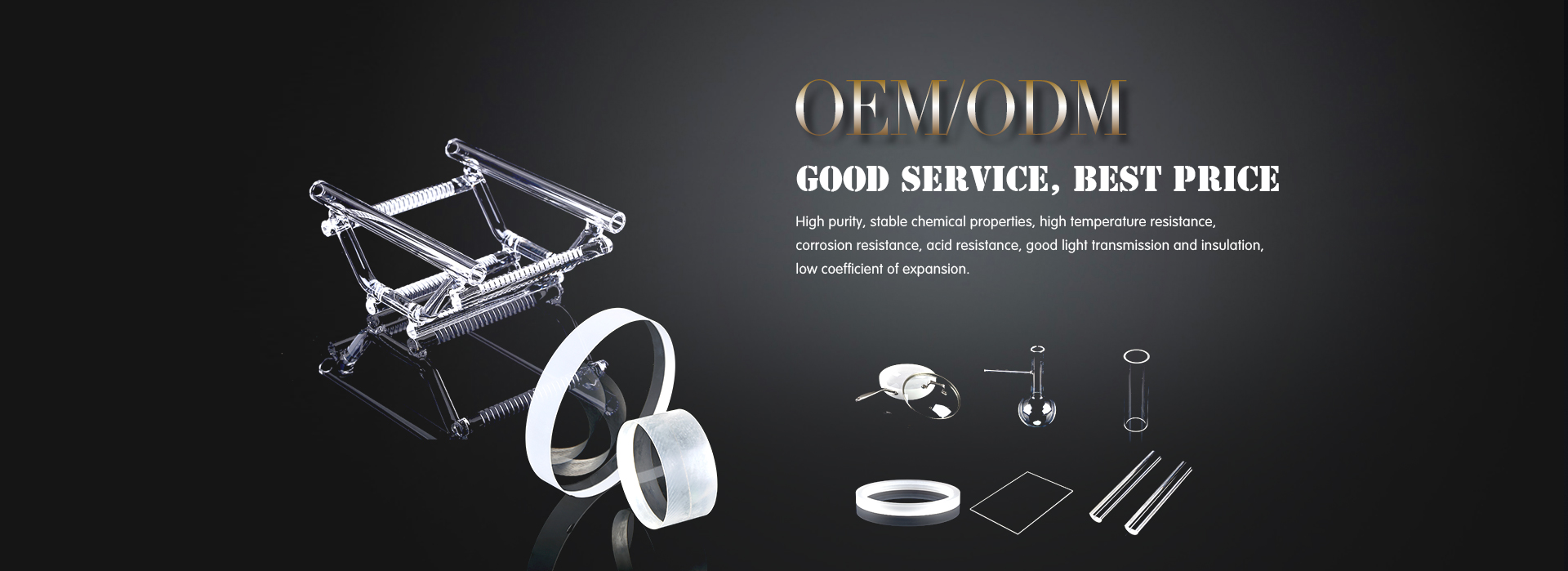
Core Semiconductor & Optical Quartzware
Tailored for Lithuania’s rigorous laser physics, high-temperature thermal diffusion, and epitaxial wafer handling systems. Every component complies with strict DIN ISO tolerances and class-leading purity benchmarks.
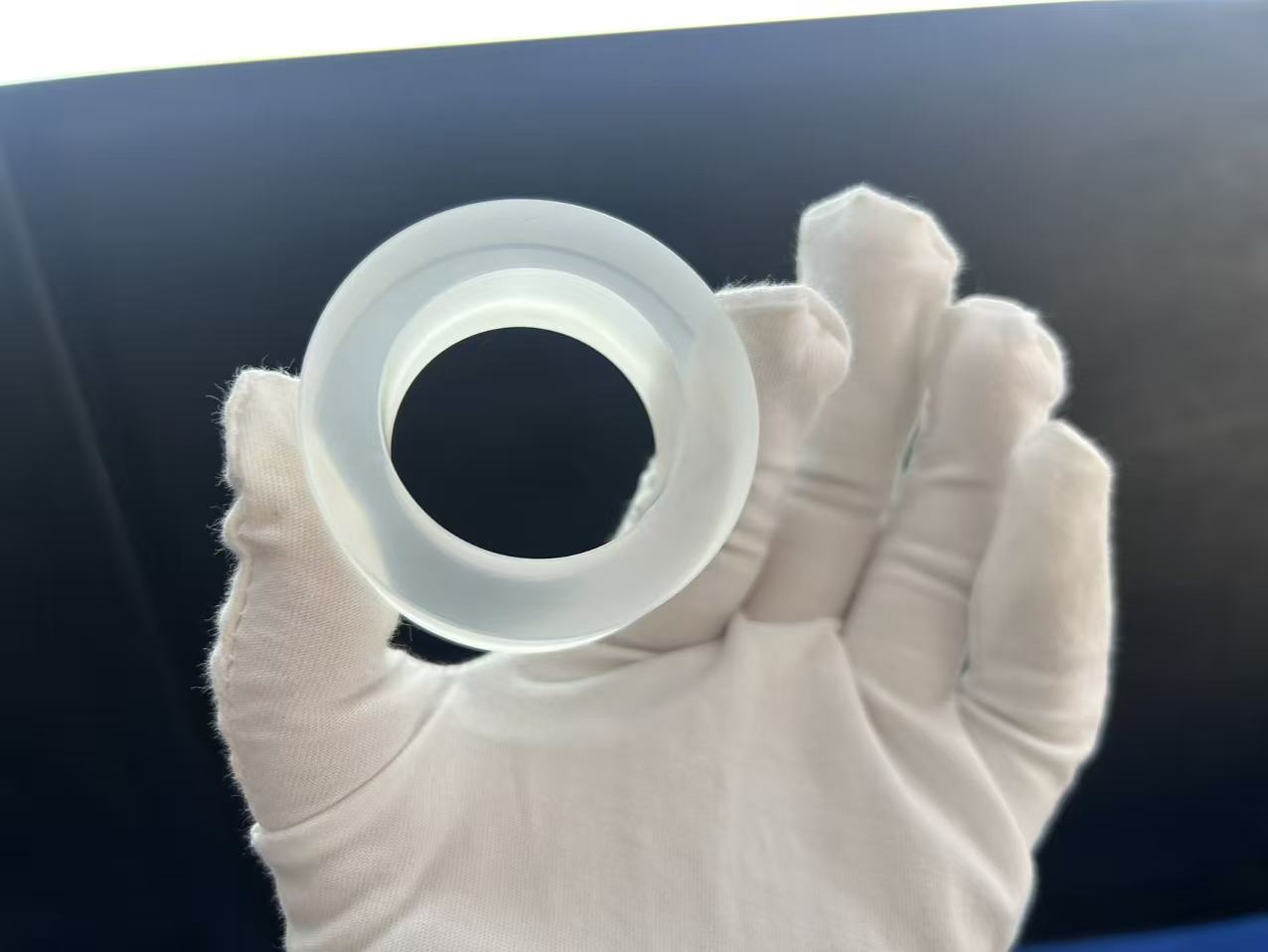
High-Precision Semiconductor Quartz Ring
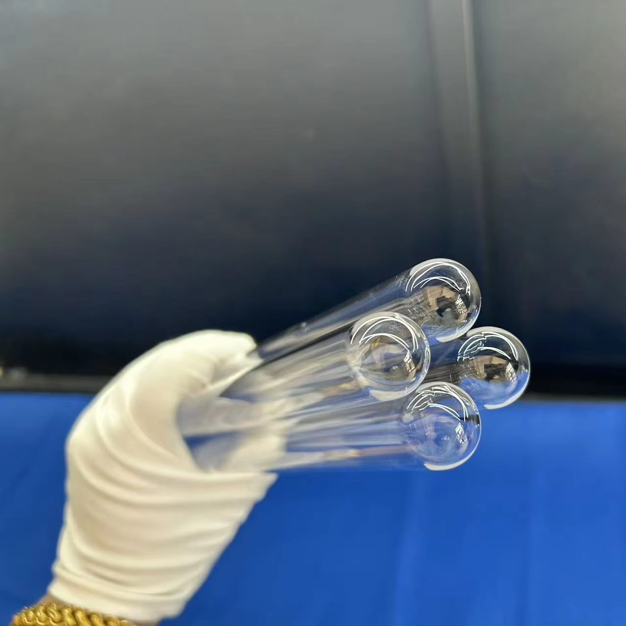
High-Purity Fused Silica Bottom Sealing Tubes (Dia 20-25mm)
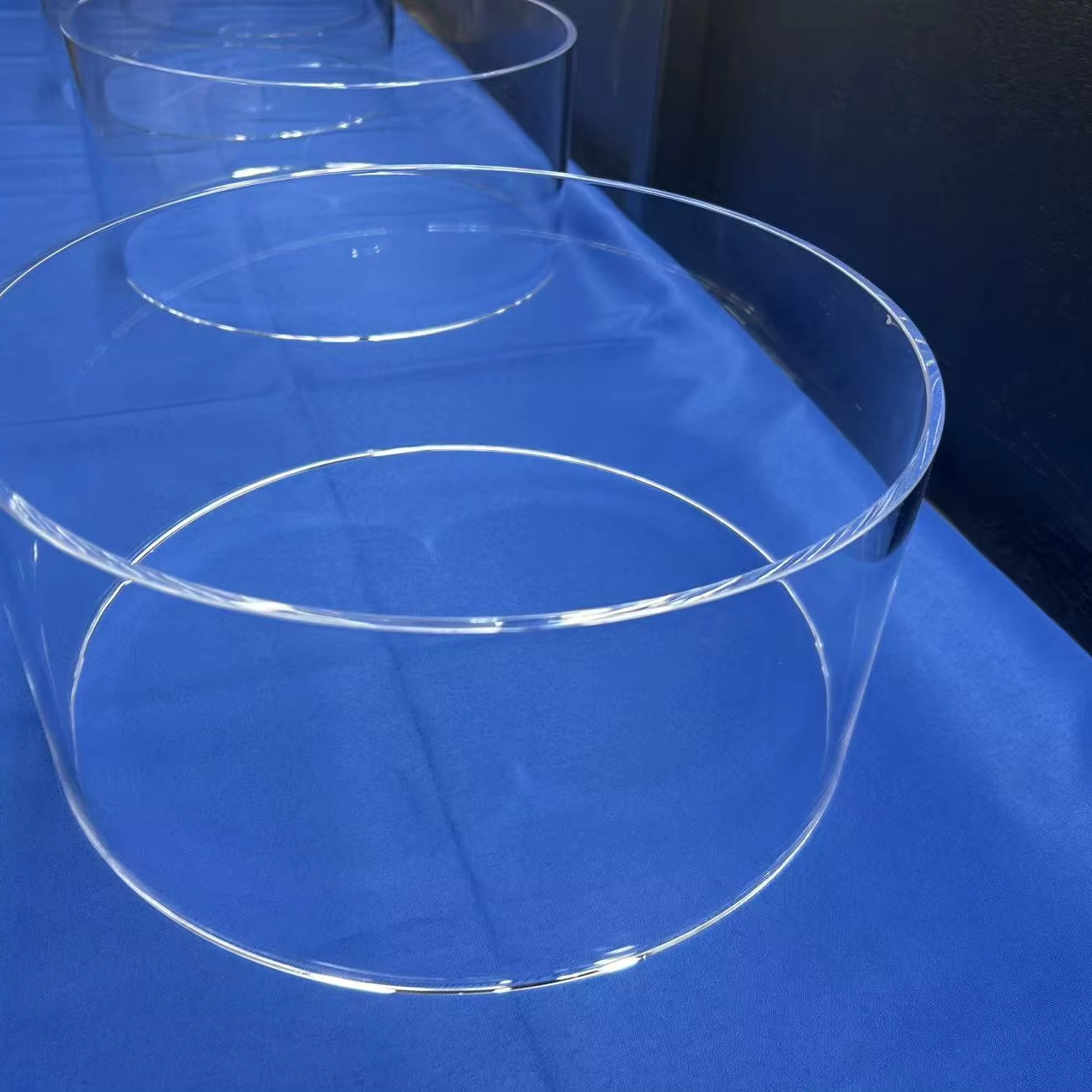
Large Diameter Fused Quartz Rods: Cutting & Bending Services
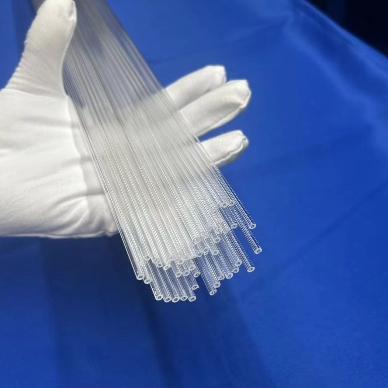
Ultra-Precision Capillary Quartz Tube for Microfluidics
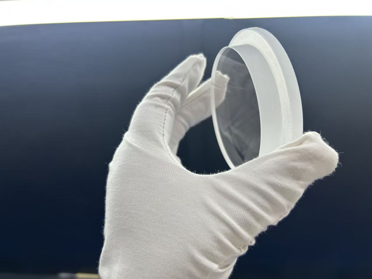
Ultra-Thick Quartz Double-Layer Step Plate with CNC Polishing
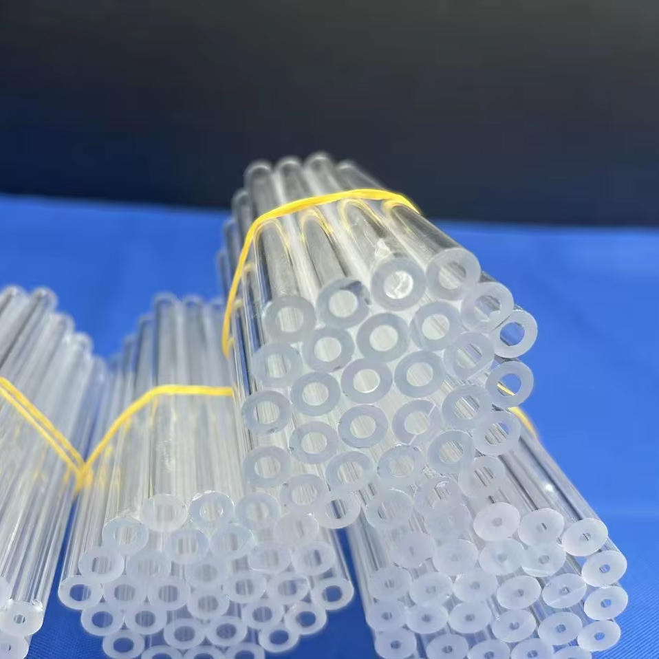
Clear Quartz Glass BET Analyzer Tube & Precision Cuvette
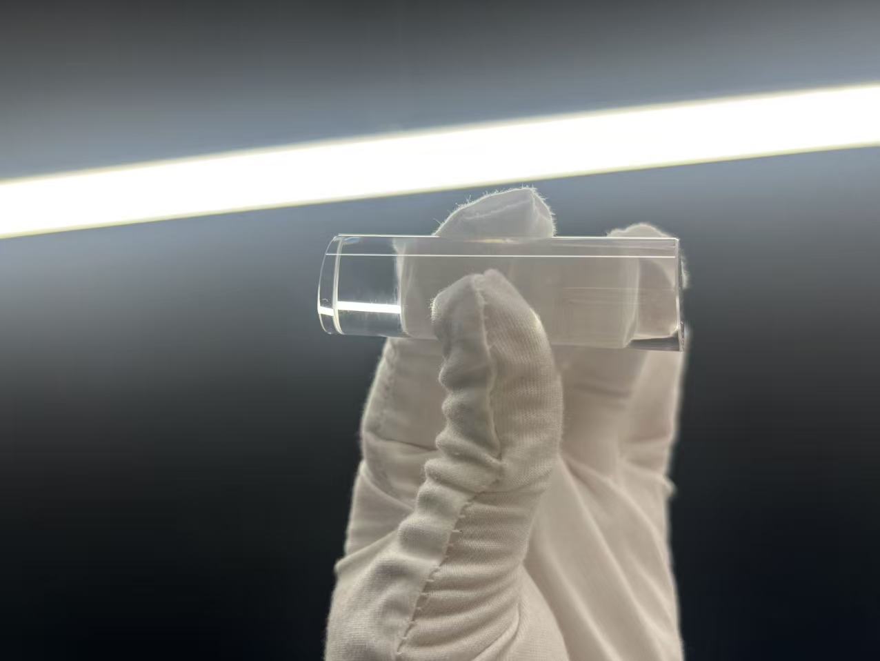
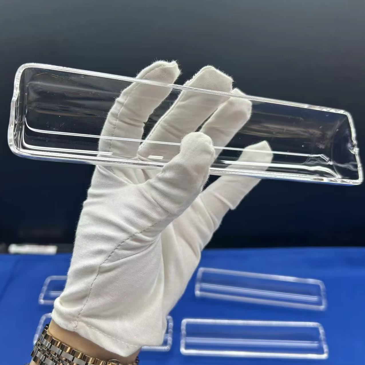
Clear Fused Silica Quartz Boat & Polished Wafer Carrier
Material Science of Synthetic & Fused Quartz Wafers
A rigorous examination of trace elemental purity, optical dispersion, laser-induced damage thresholds (LIDT), and mechanical geometry for deep-tech engineers in the Baltic region.
In high-end optoelectronic fabrication and sub-picosecond laser science—domains where Lithuanian enterprises lead worldwide—the functional substrate serves not as a passive carrier, but as an active optical element. High-purity quartz wafers (fused silica / fused quartz) are preferred over crystalline silicon, borosilicate, or optical crowns due to their phenomenal thermal shock resistance (near-zero coefficient of thermal expansion of 5.5 × 10⁻⁷ /°C), extreme optical transmission spanning from 185 nm (Deep UV) up to 3500 nm (Infrared), and extraordinary chemical resistance against aggressive acids during wet chemical etching.
At Donghai County Nivra Quartz Products Co., Ltd., based in China’s quartz synthesis hub, our engineering lines produce synthetic fused silica (JGS1), optical grade fused quartz (JGS2), and low-hydroxyl infrared transparent quartz (JGS3). Our substrates are tailored directly to European cleanroom requirements, integrating chemical-mechanical planarization (CMP) to maintain exceptional Total Thickness Variation (TTV < 1.5 μm) and minimal Bow/Warp (< 10 μm) on 2-inch, 3-inch, 4-inch, 6-inch, 8-inch, and 12-inch wafer geometries.
Lithuanian Laser Integrators Note: For high-energy ultrafast Ti:Sapphire (800 nm) and Ytterbium (1030 nm) multi-pass amplifiers, synthetic JGS1 eliminates interstitial bubble clusters and micro-inclusions down to class 0 per DIN 3140, achieving Laser-Induced Damage Thresholds (LIDT) exceeding 15 J/cm² at 1064 nm (10 ns pulse width).
| Optical / Material Grade | Synthesis / Raw Method | Useful Spectral Band | Hydroxyl (OH⁻) Content | Primary Baltic Application |
|---|---|---|---|---|
| JGS1 (Synthetic Silica) | SiCl₄ Vapor Phase Hydrolysis | 185 nm – 2500 nm (DUV-Vis) | ≥ 1200 ppm (High OH) | Femtosecond DUV optics, bio-fluorescence microchips, excimer laser windows |
| JGS2 (Optical Fused Quartz) | Purified Natural Crystal Fusion | 220 nm – 2500 nm (UV-Vis) | 30 – 150 ppm (Medium OH) | Semiconductor wafer boats, high-temperature sight glasses, solar PV carriers |
| JGS3 (Infrared Fused Silica) | Electric Vacuum Melting | 260 nm – 3500 nm (IR-SWIR) | ≤ 5 ppm (Water-free) | Optical Parametric Amplifiers (OPA), Mid-IR spectroscopy, thermal pyrometry |
| Semiconductor Fused Silica | Arc Fusion of Natural Quartz | Visible – Thermal Range | < 30 ppm | Lithography chucks, diffusion furnace tubes, plasma etch quartz rings |
Elemental purity governs both electrical insulation breakdown and UV solarization resistance. Trace metallic impurities such as Iron (Fe), Copper (Cu), and Alkali metals (Na, K, Li) create color centers and accelerate devitrification into cristobalite when subjected to prolonged temperatures above 1100°C in semiconductor diffusion and annealing chambers. Nivra Quartz guarantees total metallic impurities ≤ 15 ppm across our semiconductor wafer product lines, with ultra-pure synthetic grades reaching ≤ 0.5 ppm total metals.
| Trace Impurity Element | Typical Level - Natural Fused Quartz (ppm) | High Purity Synthetic JGS1 (ppm) | Impact on Micro-fabrication & Laser Optics |
|---|---|---|---|
| Aluminium (Al) | 8.0 – 14.0 | < 0.05 | Acts as network modifier; elevated levels trigger optical scattering centers. |
| Iron (Fe) | 0.1 – 0.5 | < 0.02 | Induces parasitic absorption in the near-UV and visible spectra; degrades LIDT. |
| Sodium (Na) / Potassium (K) | 0.5 – 1.2 | < 0.01 | Mobile alkali ions; critical threat to gate dielectric stability in MOS/CMOS lines. |
| Titanium (Ti) | 0.8 – 1.5 | < 0.01 | Shifts UV absorption edge; generates luminescence under deep-UV irradiation. |
| Calcium (Ca) / Magnesium (Mg) | 0.4 – 0.9 | < 0.03 | Promotes localized crystal nucleation during high-temperature rapid thermal processing (RTP). |
Localized Applications in Lithuania’s High-Tech Ecosystem
How Donghai County Nivra Quartz Products Co., Ltd. empowers Lithuania’s renowned photonics valleys, burgeoning semiconductor developments, and academic research institutions.
Vilnius Ultrafast Laser Valley
Lithuania manufactures over 50% of the world's scientific-grade picosecond and femtosecond lasers. Leading laser manufacturers based around Mokslininkų g., Dvarčionys, and Visoriai IT Park integrate our double-side polished (DSP) JGS1 fused silica wafers as optical delay line substrates, beam splitters, output couplers, and low-dispersion window optics where wavefront distortion cannot exceed λ/10.
Teltonika High-Tech Hill & Microchips
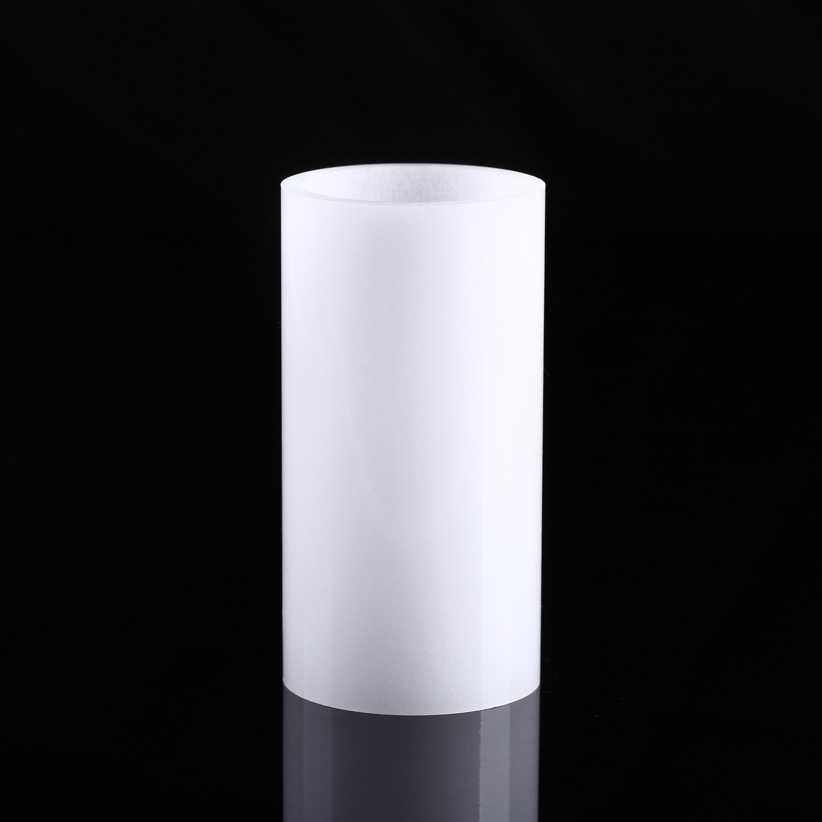
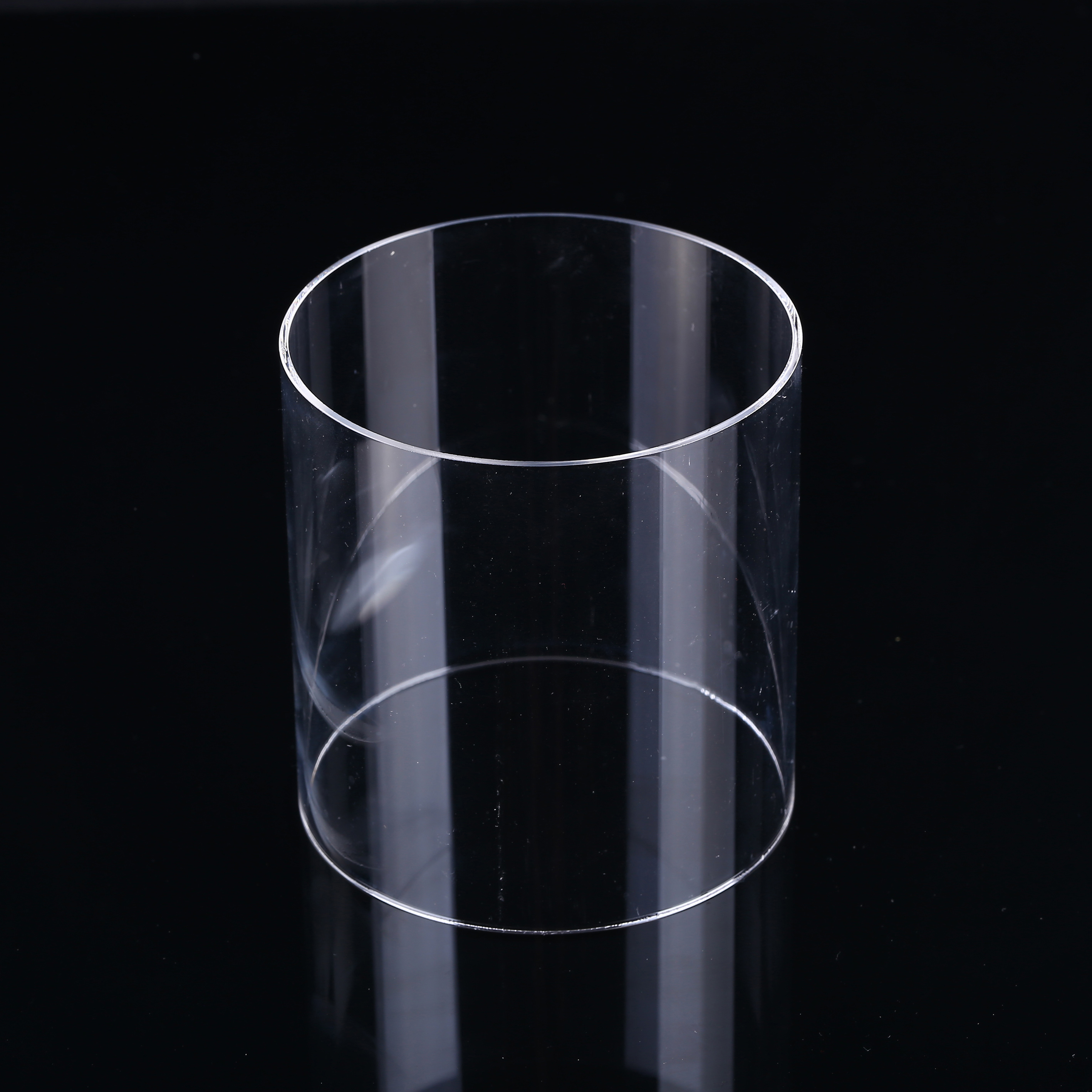
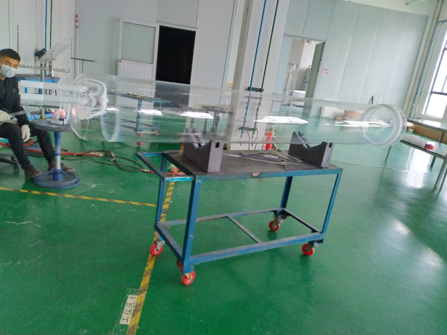
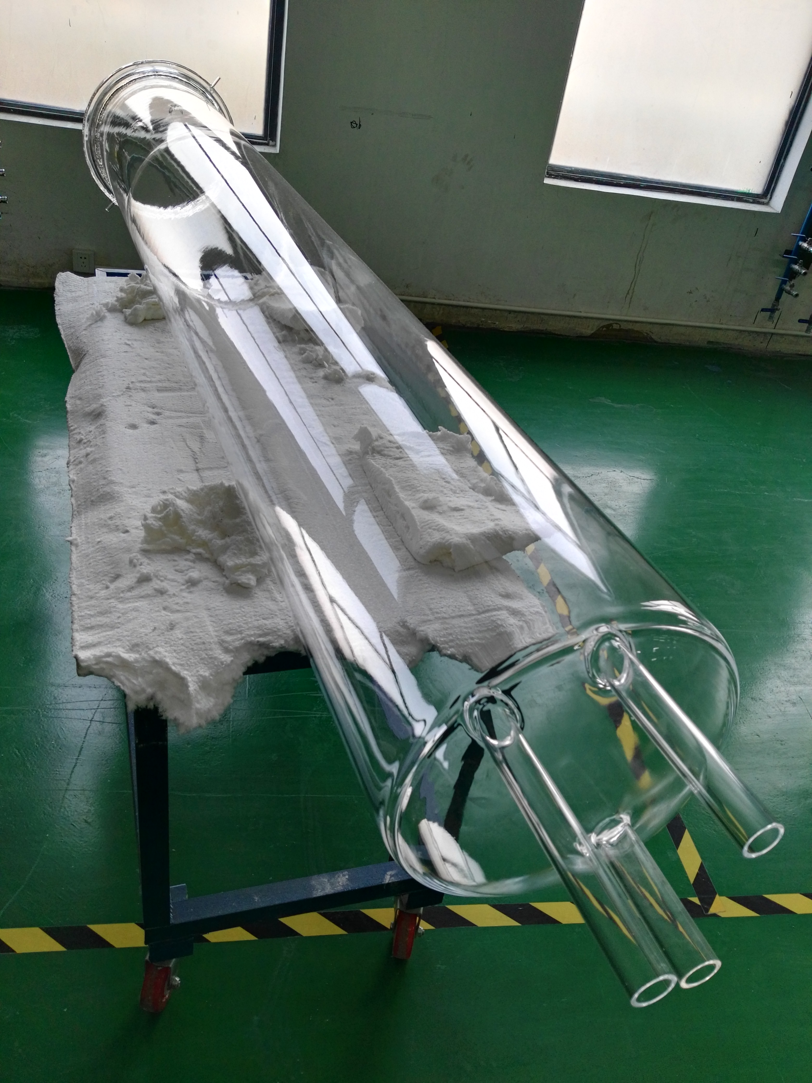
As Lithuania accelerates its landmark high-tech chip manufacturing roadmap in Liepkalnis (Vilnius), Nivra Quartz delivers OEM thermal process quartzware: large-bore diffusion furnace process tubes (up to 450 mm OD), LPCVD quartz liners, high-purity quartz wafer carriers, and quartz rings with tight geometric tolerances capable of 1200°C sustained operation without sagging or devitrification.
Bio-MEMS & Microfluidics (Kaunas & Vilnius)
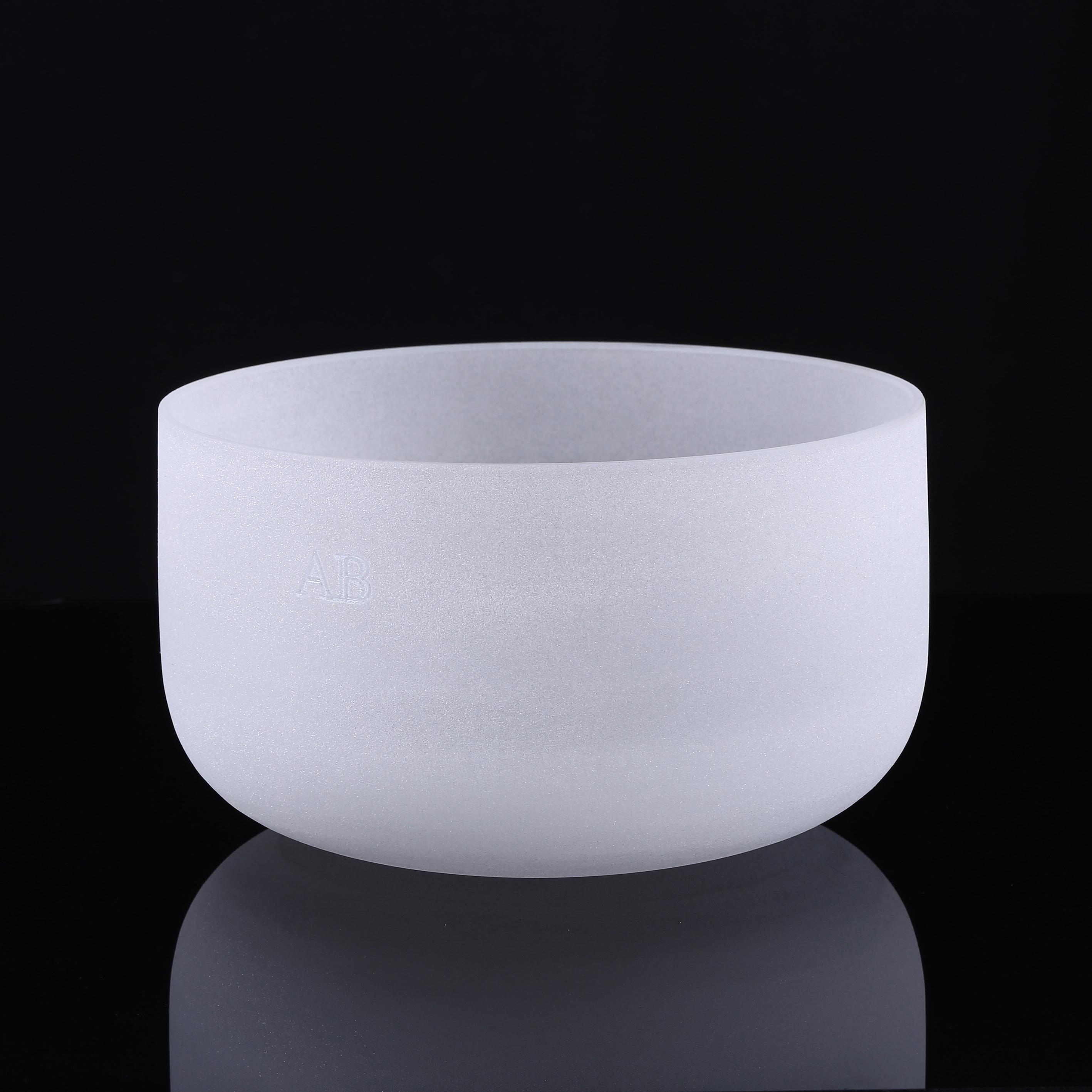
Lithuania's thriving red biotechnology cluster requires bio-compatible, ultra-transparent lab-on-a-chip substrates. Our micro-machined capillary tubes, drilled quartz wafers, and double-layer step plates allow laser-ablated microchannels for continuous-flow DNA amplification, capillary electrophoresis, and single-molecule spectroscopy with near-zero background autofluorescence.
Academic & Industrial Synergy: FTMC & VU Laser Research Center
Lithuania's Center for Physical Sciences and Technology (FTMC) and Vilnius University Laser Research Center (LRC) conduct fundamental research in nonlinear optics, high-harmonic generation (HHG), and laser-matter interactions. These elite applications require custom wafer geometries—such as ultra-thin fused silica membranes down to 70 μm thickness, stepped circular flats, and micro-grooved quartz wafers.
Nivra Quartz bridges the gap between academic prototyping and high-volume commercial scaling. By utilizing ultrasonic CNC milling and precision planetary double-sided chemical polishing, we deliver sub-angstrom surface finishes (< 3 Å RMS) to Lithuanian institutes, ensuring complete reproducibility from one experimental campaign to full-scale European production.
Strategic Trends Shaping Quartz Demand in Lithuania
Navigating technological shifts across the Baltic corridor: from EU semiconductor sovereignty to next-generation quantum optics.
The geopolitical and technological drive towards European microelectronics autonomy under the European Chips Act is fundamentally reshaping procurement strategies across the Baltics. Lithuania is positioning itself as a vital European gateway for power electronics, compound semiconductor assembly (GaN and SiC), and photonics integrated circuits (PICs). This macro shift drives three critical sourcing trends for quartz glass materials:
1. Escalation from Standard Substrates to Sub-Nanometer Planarization: As local optical workshops develop deeper-UV optical coatings and extreme harmonic generation systems, standard commercial pitch-polished wafers no longer suffice. Procurement managers are mandating Zygo-interferometer certified surface topography, with Ra < 0.2 nm and Scratch-Dig ratings of 10/5 per MIL-PRF-13830B to eliminate phase distortion and laser scattering losses.
2. Direct Sourcing from Source Synthesis Hubs: European tier-1 optical distributors often introduce 200–300% price markups and 16–24 week lead times on high-purity quartz substrates. Lithuanian laser engineering teams are increasingly establishing direct OEM/ODM supply conduits with specialized manufacturers in Donghai, Jiangsu—the epicentre of global quartz raw material processing. This direct-to-factory model compresses supply lead times down to 2–3 weeks while reducing capital expenditure on consumable wafer carriers, tubes, and polished blanks.
3. Expanding Requirements for Multi-Axis Custom Machined Quartzware: Lithuania’s advanced manufacturing sector is moving beyond basic circular wafers. There is sharp demand growth for custom-slotted quartz boats, precision CNC step-milled plates, perforated gas diffusion showerheads, and laser-core-drilled carrier discs designed to withstand corrosive reactive-ion etching (RIE) gases like CF₄, SF₆, and CHF₃.
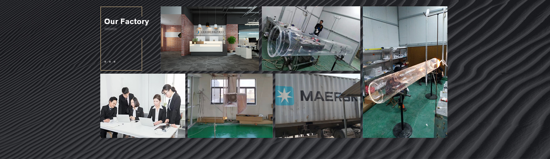
Engineered by Nivra Quartz: Donghai Precision Facility
Established in February 2019 in China’s quartz crystal capital, Donghai County Nivra Quartz Products Co., Ltd. brings together specialized manufacturing facilities, certified trade verification, and responsive engineering.
Source Material Base
Located at 285 Heping East Road, Donghai, Jiangsu. Direct access to raw high-purity silica deposits eliminates intermediaries and assures authentic material pedigree.
Full Processing Chain
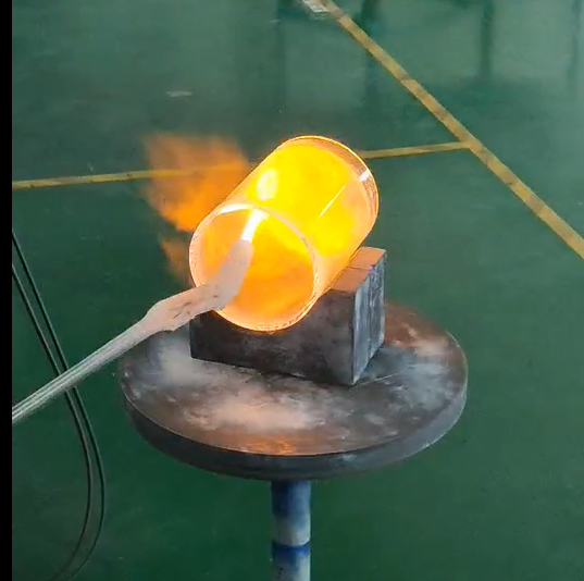
In-house CNC ultrasonic milling, diamond wire slicing, flame lathe sealing, 1200°C stress-relief annealing, and double-sided CMP polishing under one roof.
Verified Compliance
On-site audited enterprise with 101–200 specialized workers. Comprehensive quality assurance verifying dimensions, bubble classes, and surface roughness before shipment.
Rapid Baltic Logistics
Average initial engineering reply in ≤ 5 hours. Verified 88.89% inquiry response rate, custom Class 100 cleanroom packaging, and insured DDP air express to Vilnius.
Enterprise Verification & Certification Credentials
Fully registered legal corporate entity verified on-site by international inspection standards.
Lithuania Buyer FAQ: Quartz Sourcing & Compliance
Key technical, regulatory, and logistics answers for Lithuanian procurement officers, laboratory managers, and project engineers.
How do JGS1, JGS2, and JGS3 quartz wafers compare to Western equivalents (Corning 7980, Suprasil, Infrasil)?
Our grades provide equivalent optical and physical properties to standard Western designations:
JGS1 corresponds directly to synthetic fused silica grades like Heraeus Suprasil 1/2 or Corning 7980. It features high OH⁻ (800–1200 ppm) with no absorption bands in the 200–400 nm region, making it ideal for UV/DUV laser applications.
JGS2 is equivalent to Heraeus Homosil or Corning 7940 commercial grade, manufactured from natural fused quartz crystal. It provides cost-effective transmission from 260 nm to 2500 nm.
JGS3 is electrically vacuum-fused to remove hydroxyl radicals (< 5 ppm OH⁻), serving as a direct functional equivalent to Heraeus Infrasil 301/302. It eliminates the deep 2.73 μm water absorption dip, ensuring high transmittance across the near-to-mid infrared band.
What specific wafer dimensional tolerances, surface quality, and TTV can you deliver?
For semiconductor and optical substrates (50.8 mm up to 300 mm diameter), we routinely fabricate against custom technical drawings:
• Diameter Tolerance: ± 0.05 mm (precision ground) or ± 0.02 mm (CNC edged).
• Thickness Tolerance: Down to ± 0.005 mm.
• Total Thickness Variation (TTV): < 1.5 μm on 100 mm (4-inch) wafers; < 2.5 μm on 200 mm (8-inch) wafers.
• Surface Roughness (Ra): < 0.3 nm (Double Side Super Polished CMP finish).
• Scratch-Dig: 20/10 or 10/5 per MIL-PRF-13830B.
• Wafers Flats / Notches: Ground precisely per SEMI M1 standards or custom orientation flats.
How are shipments handled to Lithuania regarding customs clearance, VAT, and HS codes?
Exporting to European Union member states such as Lithuania follows harmonized EU customs frameworks. We export under standard international HS Codes:
• HS 7006.00.00: Glass plates, sheets, discs, and wafers whether or not with reflective layer.
• HS 7002.31.00: Tubes of fused quartz or other fused silica.
• HS 7017.10.00: Laboratory, hygienic or pharmaceutical glassware of fused quartz/silica.
We provide full commercial documentation: Commercial Invoices, Packing Lists with verified net/gross weights, Certificates of Origin (CO), and material purity conformity reports. Shipments to Vilnius, Kaunas, or Klaipėda can be arranged via DAP, CIF, or DDP terms with express air freight (DHL/FedEx/UPS, 4–7 business days door-to-door).
How does Nivra Quartz prevent transit breakage for fragile quartz glass products?
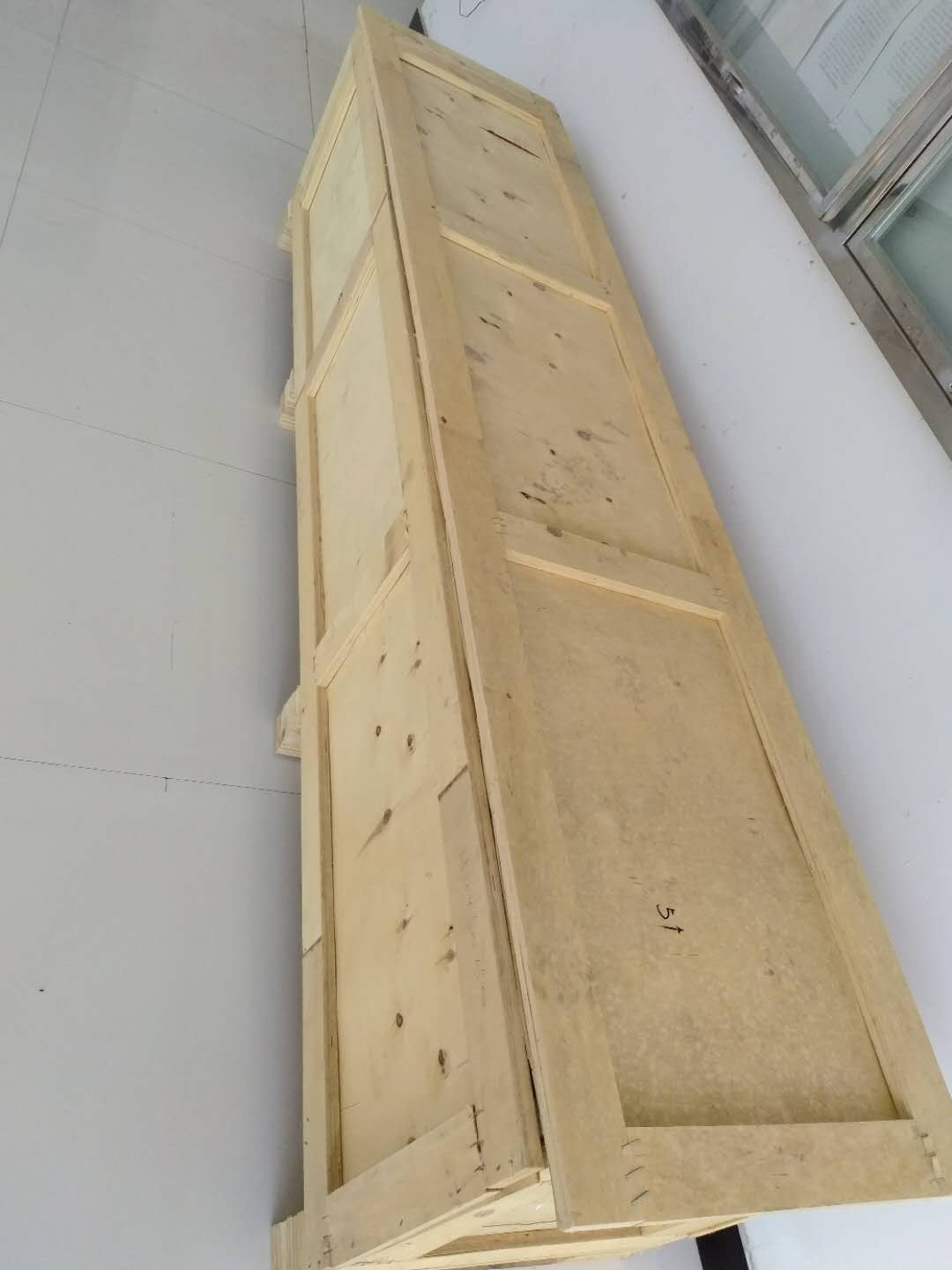
Packaging precision quartz requires rigorous shock isolation. Every polished wafer is first packed in semiconductor-grade polypropylene wafer cassettes or single-wafer fluorocarbon coin-holders within our cleanroom. Larger items—such as diffusion tubes, quartz boats, and heavy step plates—are vacuum-sealed, encapsulated in form-fitting EPE (expanded polyethylene) foam blocks, and encased in reinforced, multi-layer corrugated cartons or custom-built, fumigation-free ISPM-15 plywood export crates.
What is your Minimum Order Quantity (MOQ) for prototypes versus production batches?
We actively support academic and industrial R&D spin-offs across Lithuania. For standard circular fused quartz wafers and laboratory plates, the MOQ is 10 pieces (or 1 to 5 pieces for large customized furnace tubes, bell jars, or custom step plates). For dedicated production runs, batch volumes scale up to thousands of units with volume-tiered pricing.
What documentation is provided to guarantee compliance with EU RoHS and REACH regulations?
High-purity fused silica (SiO₂) is an inorganic glass that inherently satisfies EU Directive 2011/65/EU (RoHS) and Regulation (EC) No 1907/2006 (REACH). We supply formal declarations of conformity alongside elemental spectrographic test reports verifying that no hazardous SVHC (Substances of Very High Concern) or restricted heavy metals exceed EU threshold limits.
Ready to Accelerate Your Lithuanian Photonics or Semiconductor Program?
Upload your technical CAD drawings, wafer specifications, or thermal quartzware bill of materials. Our factory engineering team in Donghai reviews manufacturability and returns formal quotations within 5 business hours.