Standard & Custom Fabricated High-Purity Quartz Solutions
From single-side polished wafers and double-sided micro-optics to specialized high-temperature reaction tubes and labware. Explore our primary export products engineered to sub-nanometer surface roughness tolerances.
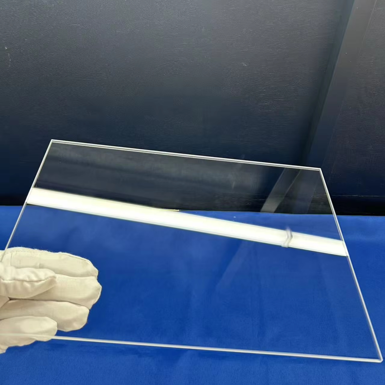
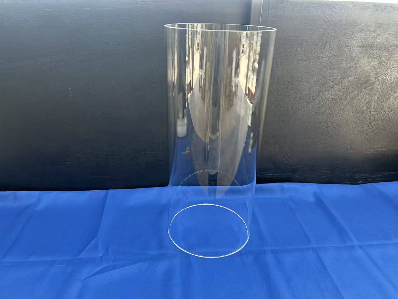
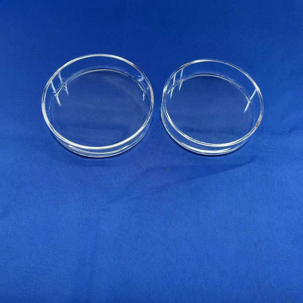
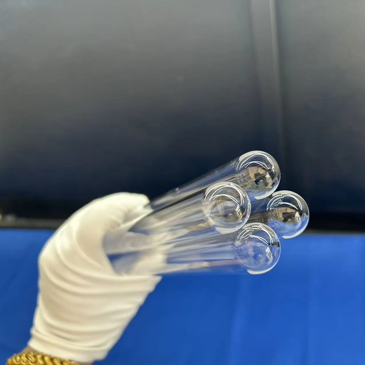
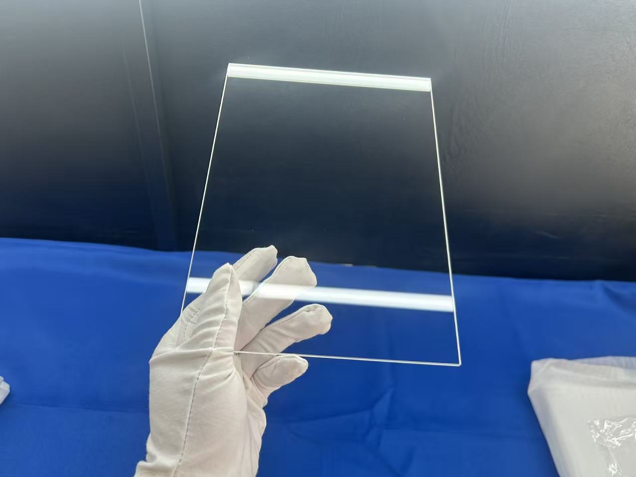
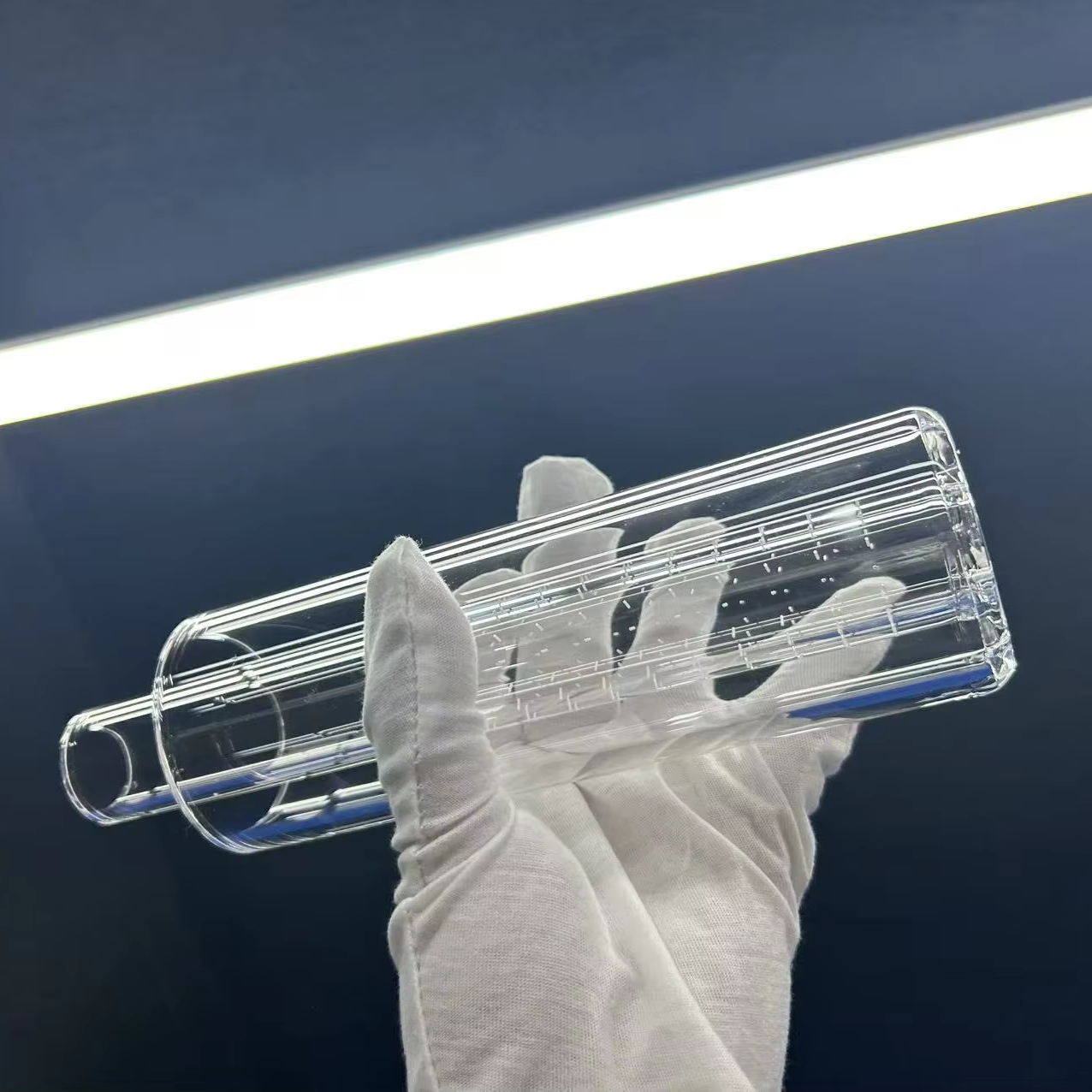
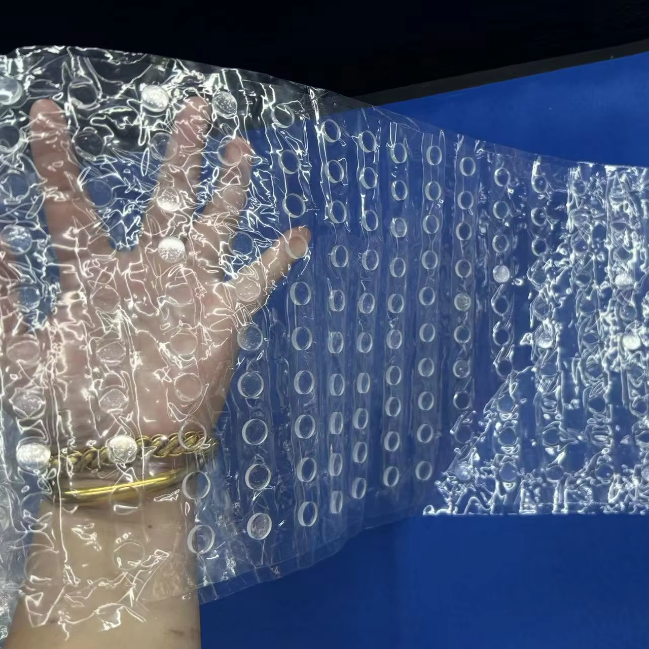
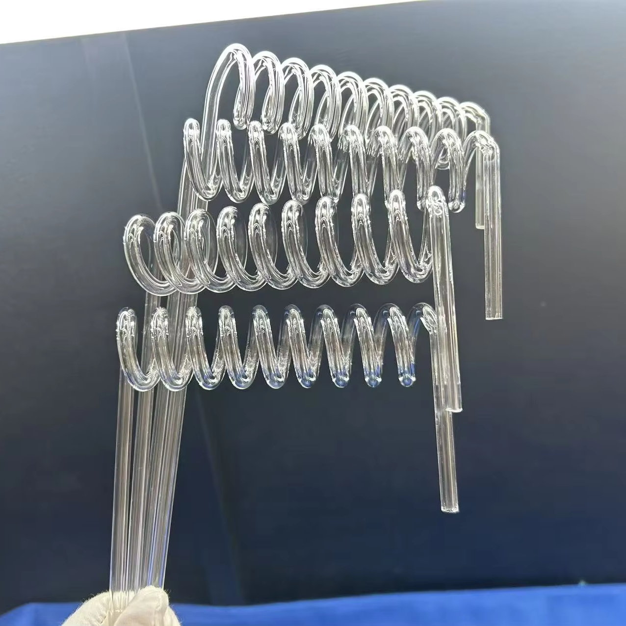
Engineering Fundamentals of High-Purity Quartz Substrates & Wafers
An in-depth metallurgical and micro-fabrication guide covering crystallographic purity, optical grade classifications (JGS1, JGS2, JGS3), and Chemical-Mechanical Planarization (CMP) standards for European cleanrooms.
High-purity fused silica and quartz wafers represent the structural and optical backbone of modern high-frequency microelectronics, MEMS (Micro-Electro-Mechanical Systems), integrated microfluidics, and deep-UV photonic circuits. In state-of-the-art European research clusters, such as those situated within the Principality of Monaco and the surrounding Côte d'Azur technology corridors, demand has evolved beyond conventional silicate glass toward defect-free, trace-metal-depleted fused quartz substrates that provide extraordinary thermal resilience, broad-band electromagnetic transmittance, and unmatched dielectric isolation.
At Donghai County Nivra Quartz Products Co., Ltd., we utilize ultra-refined natural silica sand and synthetic gaseous silicon tetrachloride (SiCl4) pre-forms to fabricate quartz substrates exhibiting silicon dioxide (SiO2) purity levels of 99.99% to 99.9999%. By mitigating ionic contaminants such as Aluminum (Al < 15 ppm), Iron (Fe < 0.2 ppm), Lithium (Li < 0.5 ppm), and Sodium (Na < 0.5 ppm), our wafers eliminate parasitic dielectric absorption, resist devitrification under sustained 1100°C furnace exposures, and guarantee exceptional surface electrical resistivity exceeding 1018 Ω·cm at ambient conditions.
Optical Grade Classifications: Synthetic Fused Silica vs. Natural Fused Quartz
Specifying the optimal substrate requires precise matching between the operating electromagnetic spectral band and the molecular hydroxyl (OH-) concentration of the quartz matrix. Our manufacturing plant categorizes precision plates and wafers into three distinct optical standards conforming to international DIN/ISO and SEMI specifications:
JGS1: Synthetic Deep-UV Grade
Produced via chemical vapor deposition flame hydrolysis. Free from bubble inclusions (Class 0). Transmission range spans 185 nm to 2500 nm, displaying virtually no solarization or luminescence under excimer laser (193 nm ArF, 248 nm KrF) radiation. High OH content (~800-1200 ppm).
JGS2: Fused Quartz UV-Vis Grade
Fired by electro-fusion from pure crystalline pegmatite quartz gravel. Excellent transparency across 220 nm to 2500 nm. Standard industry selection for optical windows, high-pressure sight glasses, lithography alignment masks, and plasma etching quartz viewports. OH content < 200 ppm.
JGS3: Low-OH Infrared Grade
Synthesized in vacuum fusion or electric resistance environments to virtually eliminate the 2.73 μm fundamental water absorption dip. Extends spectral transmission from 260 nm to 3500 nm. Preferred for mid-IR optical spectroscopy, defense optics, and cryogenic sensor thermal isolators (OH < 5 ppm).
Substrate Geometries, CMP Polishing & Cleanroom Metrology
To satisfy the demanding requirements of direct wafer bonding, optical lithography, and anodic encapsulation with silicon, Nivra Quartz maintains high-precision diamond multi-wire slicing rigs and planetary double-sided chemical-mechanical polishing (CMP) platforms. Every wafer is subjected to strict geometric validation:
| Wafer Metric | Standard Commercial Grade | Semiconductor Prime Grade | Ultra-Precision Optical Polish |
|---|---|---|---|
| Available Diameters | 2", 3", 4" (50.8 mm - 100 mm) | 100 mm, 150 mm, 200 mm (Up to 300 mm) | Custom Shapes / 10 mm to 450 mm Wafers |
| Thickness & Tolerances | 0.5 mm ± 0.05 mm | 0.35 mm ± 0.015 mm / Custom ± 0.005 mm | Down to 0.15 mm ± 0.003 mm ultra-thin |
| Total Thickness Variation (TTV) | ≤ 10 μm | ≤ 3 μm | ≤ 1.5 μm (Interferometrically verified) |
| Surface Roughness (Ra) | ≤ 1.5 nm | ≤ 0.5 nm (CMP Both Sides) | ≤ 0.2 nm – 0.3 nm (Super-polished) |
| Bow / Warp | ≤ 25 μm | ≤ 15 μm | ≤ 8 μm |
| Surface Scratch-Dig (MIL-PRF-13830B) | 60/40 | 40/20 | 20/10 or 10/5 (Laser substrate quality) |
| Edge Profile & Orientation Flats | Ground C-shape bevel; single flat | SEMI standard flat / notch rounded edge | Fully laser-marked & fire-polished chamfer |
* Custom diameter slicing, customized laser profiling, ultrasonic drilled micro-vias (Ø ≥ 0.2 mm), and vacuum-sealed Class 100 cleanroom packaging provided upon request.
Localized Application Scenarios in Fontvieille & the Riviera Tech Hub
Fontvieille is Monaco’s premier technological engine, integrating high-density cleanroom facilities, advanced pharmaceutical laboratories, marine optronics research, and micro-precision mechanics.
Biomedical Analysis & Microfluidics
Fontvieille’s prominent life sciences cluster develops micro-electrochemical assays, flow cytometry chambers, and lab-on-a-chip cartridges. High-purity quartz provides non-autofluorescent optical clarity, biocompatibility, and utter chemical inertness against harsh solvents, enabling zero-drift spectroscopic quantification.
Luxury Horology & Micro-Mechanics
Monaco’s elite engineering ateliers craft high-complication timepieces and micro-mechanical regulators. Chemically etched and precision-lapped quartz plates act as frictionless kinematic bridges, transparent inspection crystals, and thermal-expansion-free structural baselines that operate reliably across volatile marine environments.
Aerospace & Satellite Optronics
In collaboration with the nearby Sophia Antipolis aerospace nodes, Fontvieille subcontractors design miniaturized satellite star trackers, LIDAR viewports, and payload mirrors. Our low-bubble JGS1 substrates offer high radiation tolerance, vacuum outgassing ratings of zero, and near-zero coefficient of thermal expansion (5.5 × 10⁻⁷/°C).
Marine Ecology & Subsea Sensors
Supporting oceanographic initiatives guided by the Oceanographic Institute and local superyacht tech providers, heavy-wall quartz bottom-sealing tubes and thick fused silica sight ports endure hydrostatic deep-sea pressures over 600 bar, providing high UV-VIS transparency for deep-ocean fluorometric sensors.
Trends Reshaping High-Purity Quartz Procurement in Monaco
As Fontvieille cleanrooms modernize to align with European Green Deal directives and micro-electronics scaling, procurement criteria have transitioned from commodity buying to deeply customized OEM engineering partnerships.
1. High-Density Photonic-Electronic Convergence
With local micro-electronic designs moving toward optical interconnects and quantum key distribution (QKD), wafer specifications demand Total Thickness Variation (TTV) ≤ 1.5 μm and roughness Ra ≤ 0.2 nm. Synthetic JGS1 wafers serve as passive optical interposers, supporting high-throughput waveguiding and direct dielectric-to-dielectric wafer bonding.
2. Decarbonized & Traceable Supply Chains
Monaco’s national commitment to Carbon Neutrality by 2050 compels Fontvieille manufacturing enterprises to audit Scope 3 lifecycle emissions. Nivra Quartz supports these imperatives by using hydro-electric powered refining furnaces, 100% recyclable mineral-based packaging, and comprehensive material traceability documentation compliant with REACH/RoHS.
3. Agile Prototyping & Sub-50 MOQ Delivery
Unlike rigid mega-foundries enforcing minimum runs of thousands of units, European specialty engineering requires boutique batches (10 to 500 units) for rapid design validation. Nivra Quartz bridges this divide with quick-turn laser profiling, no costly tooling charges, and rapid air express transit to Nice Côte d’Azur International Airport (NCE).
Procurement Insight for Fontvieille Cleanroom Managers
When ordering quartz wafers destined for French/Monegasque customs handling under TARIC HS Code 7002.31 / 7006.00, engineering specifications must detail crystallographic axis orientation (for crystalline quartz) versus amorphous fused silica, hydroxyl band limits, and class cleanness certs to streamline entry through the Nice Port-de-Saint-Laurent / Monaco border control without customs hold-ups.
Donghai Nivra Quartz: Factory-Direct Strength & Precision Control
Headquartered in Donghai County, China's world-renowned quartz capital, Donghai County Nivra Quartz Products Co., Ltd. operates as a specialized manufacturer and trading entity with 101–200 employees, merging raw silica reserves with precision CNC micro-machining.
Precision Fabrication Lifecycle: From Ingot to Cleanroom Delivery
Raw Refining
High-temperature vacuum fusion of ≥99.99% pure silica into homogeneous, bubble-free cylindrical ingots.
Wire Saw Slicing
Diamond multi-wire cutting yields wafer blanks with nominal thickness kerf loss and reduced micro-cracking.
CNC Lapping & Edging
Precision edge chamfering, SEMI notch creation, and double-sided planetary abrasive planarization.
CMP Optical Polish
Multi-stage colloidal cerium/silica oxide polishing achieving super-flat surfaces with Ra < 0.5 nm.
Cleanroom Inspection
Zygo laser interferometry, ultrasonic bath cleaning, and individual anti-static vacuum sealed packaging.
Direct Source Economics
Direct access to Donghai’s crystalline silica reserves eliminates intermediate brokerage, slashing raw material procurement overheads by 20% to 35% without purity compromises.
≤ 5h Rapid Response
Our multilingual engineering desk boasts an 88.89% inquiry response rate, delivering drawing assessments, tolerancing feedback, and production quotes within 5 hours for European time zones.
Zero-Breakage Packaging
Every substrate is individually wrapped in cleanroom wafer cassettes, cushioned by customized shock-absorbing EPE foam, and encased within export-ready fumigated timber containers.
Complete OEM/ODM Scope
From micro-drilling, flame polishing, and precision lathe tube bending to metal-to-quartz sealing and sapphire window integration, consolidate all optical glass components under a single audited supplier.
Frequently Asked Questions for Fontvieille & European Buyers
Essential clarifications regarding import logistics to Monaco, optical tolerances, testing protocols, and custom drawing capabilities.
How do you manage international shipping, customs, and delivery into Fontvieille, Monaco?
Shipments destined for Fontvieille entities (or Sophia Antipolis technology parks) are dispatched via air express (DHL, FedEx, UPS) or freight forwarders routed into Nice Côte d’Azur International Airport (NCE), located just 30 km from Fontvieille. Deliveries are cleared under Franco-Monegasque customs union regulations without additional regional duties. All paperwork, including Certificates of Conformance (CoC), EUR.1 declarations, commercial invoices, and packing manifests with exact HS codes (e.g., 7002.31 for fused quartz tubes, 7006.00 for worked wafers), are supplied for immediate clearance.
What is the fundamental optical transmission difference between JGS1, JGS2, and JGS3 grades?
JGS1 is synthetic fused silica optimized for deep-ultraviolet (DUV) applications (185 nm – 2500 nm), exhibiting zero bubble inclusion (Class 0) and high laser-induced damage thresholds. JGS2 is standard optical fused quartz providing robust transmission in the UV-to-visible spectrum (220 nm – 2500 nm), making it cost-effective for sight glasses, plasma chambers, and general optical flats. JGS3 is an infrared-grade silica formulated in a vacuum environment with ultra-low hydroxyl (OH < 5 ppm), extending the transmission band smoothly out to 3500 nm without water absorption drops at 2.73 μm.
Can Nivra Quartz manufacture custom substrates directly from customer CAD drawings?
Yes. Over 75% of our export output involves custom fabrication. We accept 2D drawings in PDF/DXF format and 3D CAD files in STEP/IGES format. Our engineers analyze dimensional tolerances, hole patterns, chamfers, edge bevels, and surface roughness requirements. Engineering feedback, DFM (Design for Manufacturability) advice, and fixed quotation packages are returned within 5 hours.
What are the minimum order quantities (MOQ) for custom quartz wafers and components?
To support advanced R&D centers, medical equipment startups, and specialty watchmakers in Fontvieille, we maintain low MOQs. Standard optical plates, tubes, and large crucibles can be ordered from 1 to 10 pieces. Precision micro-wafers, thin discs, and CNC-drilled parts typically start at 25 to 50 pieces, with prototype evaluation units readily supplied prior to volume batch runs.
How do you prevent micro-cracking and particle contamination during transcontinental shipping?
Following final optical inspection, each quartz wafer undergoes multi-stage ultrasonic degreasing in deionized water and is sealed inside dust-free cleanroom single-wafer coin boxes or multi-wafer fluoroware-style cassettes. Cassettes are vacuum-sealed in nitrogen-flushed anti-static metallized bags and protected by custom high-density polyethylene (EPE) shock dampeners in reinforced corrugated boxes or fumigation-free wooden crates.
What thermal thresholds and thermal shock limits do your fused silica materials withstand?
Our clear fused quartz exhibits a softening point at approximately 1683°C, an annealing point at 1215°C, and a continuous operating rating of 1100°C (short-term excursions up to 1450°C). Due to an exceptionally low coefficient of thermal expansion (α = 5.5 × 10⁻⁷/°C between 20°C and 320°C), our quartz components can be heated to 1000°C and rapidly quenched in cold water without cracking or thermal shock spalling.
Ready to Accelerate Your High-Purity Quartz Project?
Whether you require prototype JGS1 optical wafers, large-diameter CVD diffusion furnace tubes, or micro-machined quartz plates for Fontvieille's cleanroom industries, submit your drawings or technical parameters today for an expedited engineering review.