Navigating High-Purity Quartz Wafer Solutions in Aalborg
As the Nordic industrial hub transitions toward advanced green energy, telecommunications, and photonics, the demand for semiconductor-grade high purity quartz wafers has surged exponentially in the Aalborg market. Donghai County Nivra Quartz Products Co., Ltd. delivers factory-direct engineering excellence, matching rigorous European metallurgical and optical standards.
Advanced CNC & Polishing
State-of-the-art diamond cutting, ultrasonic drilling, and optical surface polishing down to Angstrom-level roughness for optimal wafer flatness.
Deep UV & IR Transmission
Stringent grade control spanning JGS1, JGS2, and JGS3 standards to guarantee zero inclusion and exceptional optical transmission spectra.
Shock-Absorbent Logistics
Specialized export-grade packaging utilizing medical foam and fumigation-free wooden crates tailored for secure transit into Northern Europe.
Core Product Series & Precision Quartz Lineup
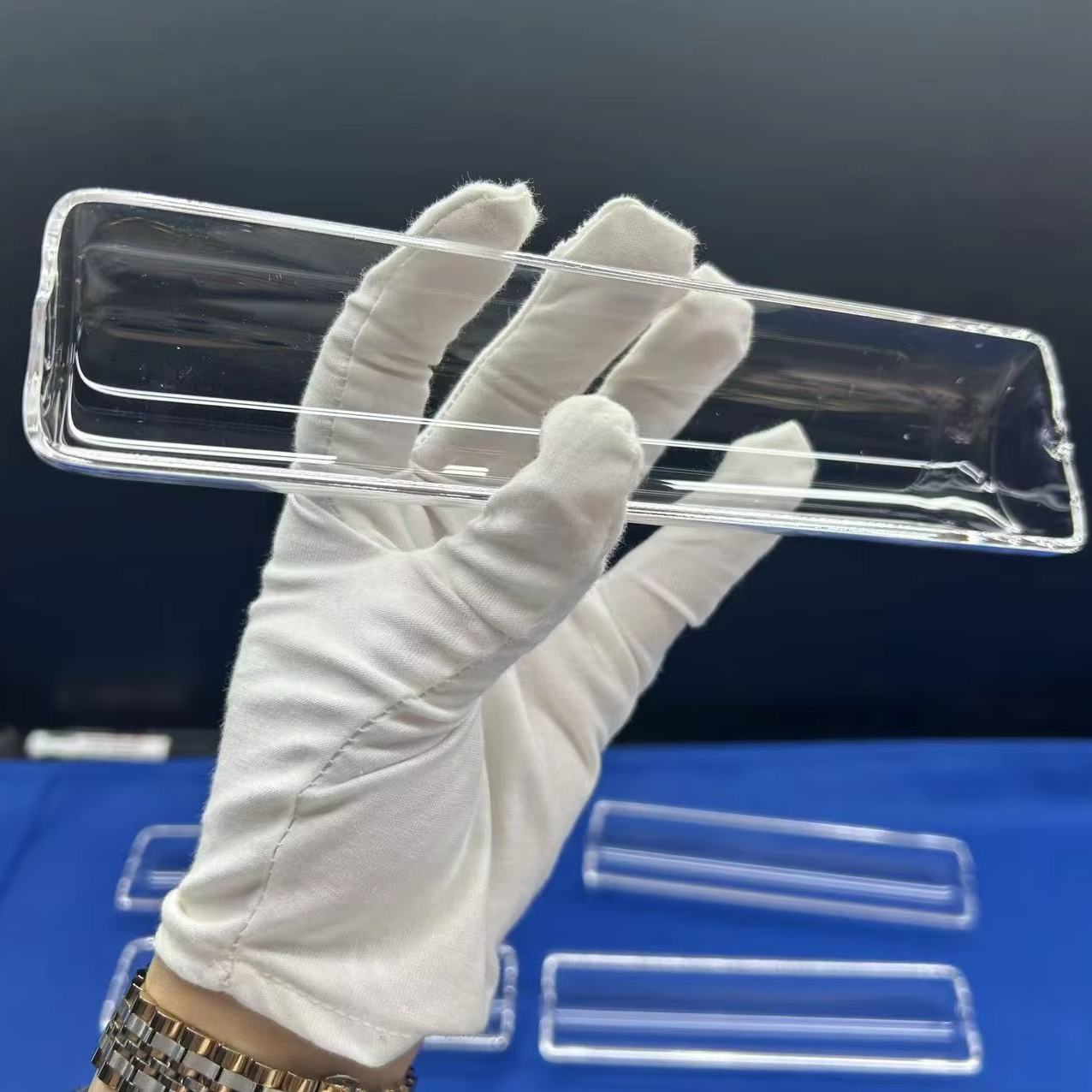
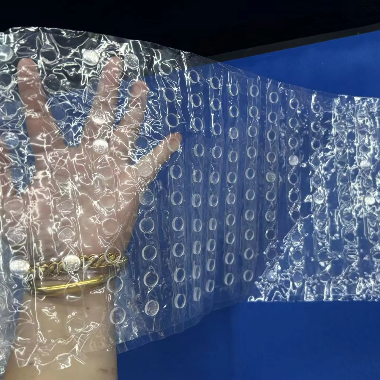
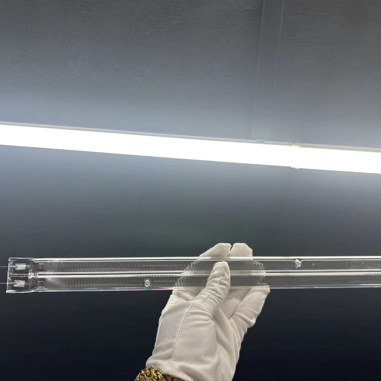
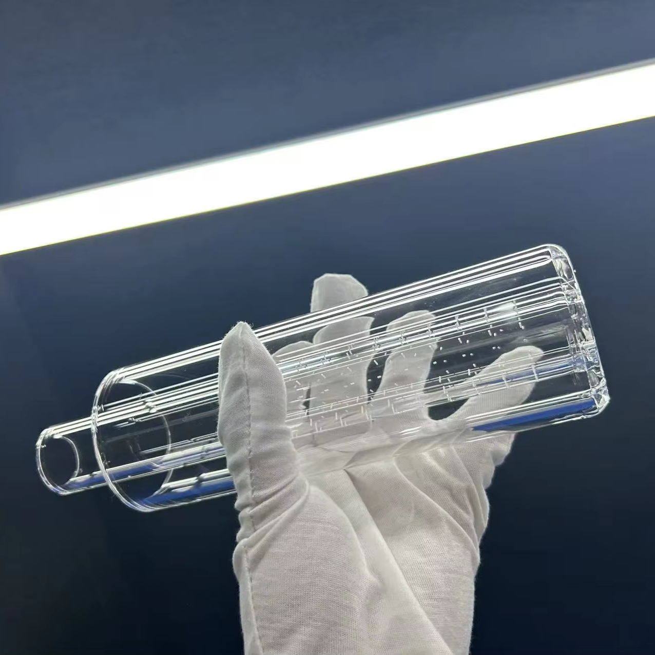
Explore our factory's direct product offerings, engineered for high-temperature resistance, thermal shock stability, and extreme chemical purity.
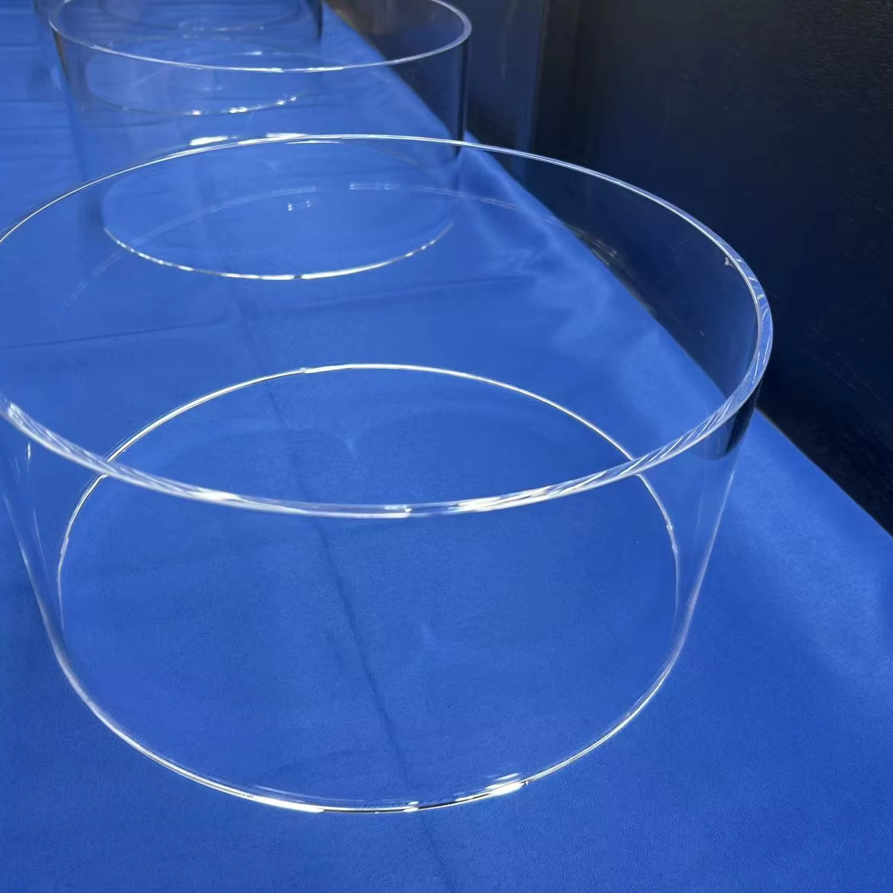
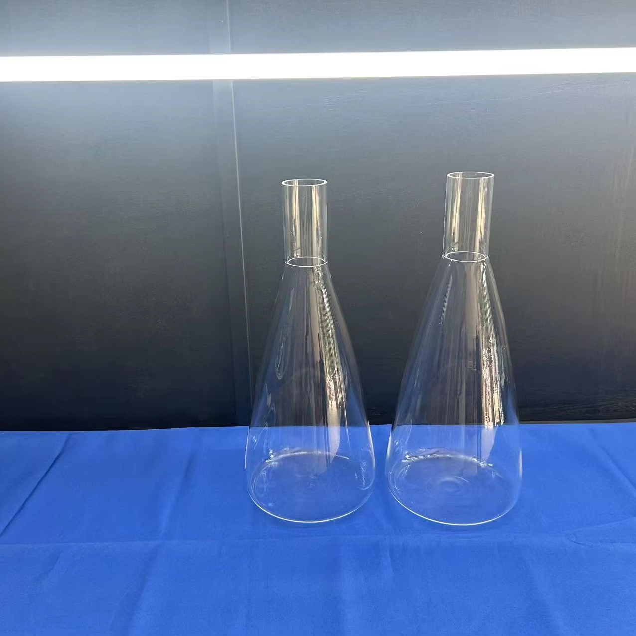
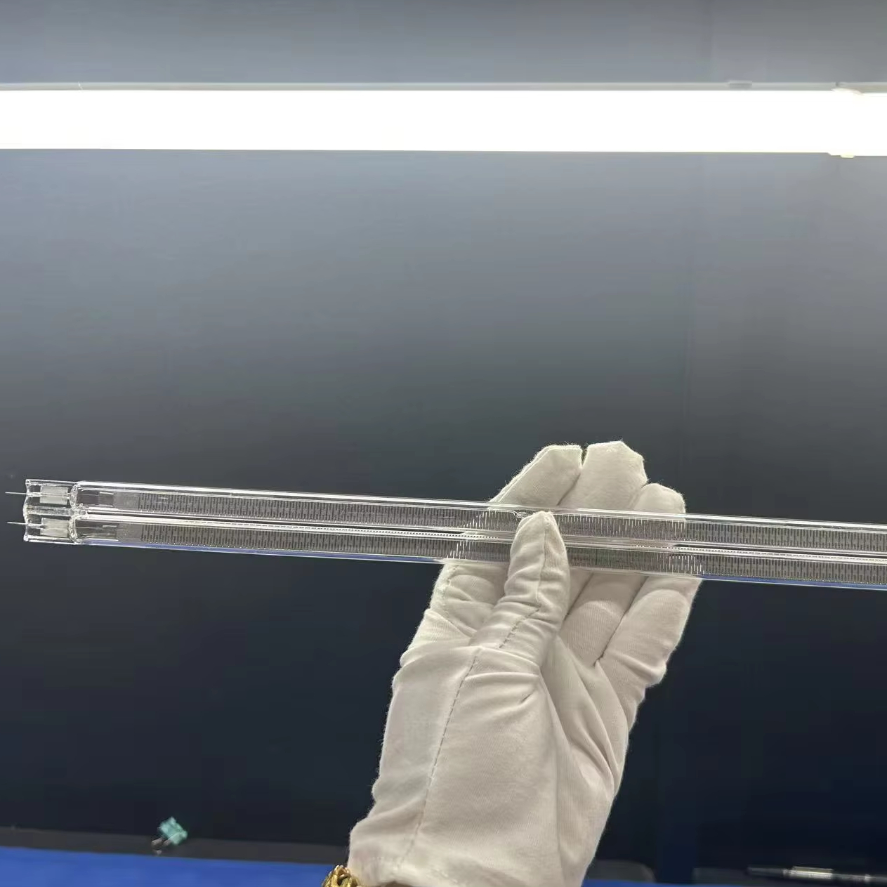
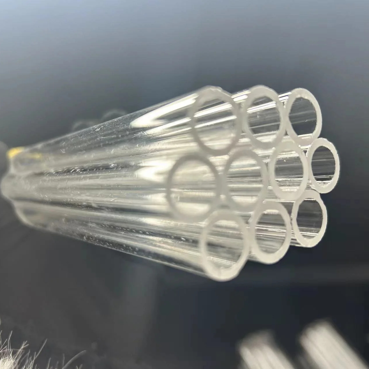
Deep Dive: High Purity Quartz Wafers in Localized Industrial & Research Ecosystems
The Aalborg market represents an increasingly vital nexus for advanced engineering, renewable energy technology, and photonics research in Northern Europe. Industrial facilities, university laboratories, and high-tech manufacturing plants in this region demand extreme material purity, exceptional thermal stability, and tight dimensional tolerances. High purity quartz wafers and optical quartz components serve as the foundational substrate for semiconductor processing, specialized laser optics, high-temperature furnace calibration, and advanced chemical reactors.
Localized Application Scenarios in Northern Europe
Procurement managers and R&D engineers across the region deploy high-purity quartz wafers in diverse operational environments:
- Semiconductor & Microelectronics Fabrication: Used as test wafers, diffusion carriers, and protective optical shields during high-temperature thermal oxidation and chemical vapor deposition (CVD).
- Renewable Energy & Photovoltaics: Serving as high-temperature substrates and diffusion boat components for solar cell manufacturing equipment.
- Laser & Optical Metrology: Providing ultra-flat optical windows (JGS1 synthetic fused silica) that maintain minimal wave-front distortion across deep ultraviolet (DUV) and infrared spectra.
- Analytical & Chemical Laboratories: Utilizing custom quartz beakers, crucibles, and microfluidic reaction tanks that resist aggressive acids and extreme thermal shock cycles.
Localized Development Trends & Sourcing Strategy
As supply chain resilience becomes a top priority for European enterprises, buyers are shifting away from rigid distribution intermediaries toward trusted direct manufacturers in established quartz hubs like Donghai, Jiangsu. By collaborating directly with Donghai County Nivra Quartz Products Co., Ltd., Aalborg-based enterprises benefit from complete transparency, custom prototyping capabilities, strict drawing compliance, and highly competitive factory-direct pricing without sacrificing strict international quality benchmarks.
Frequently Asked Questions (FAQ) for Aalborg Buyers
Answers to common technical, logistical, and commercial inquiries regarding high purity quartz wafer procurement.
What are the key technical specifications of your high purity quartz wafers?
Our quartz wafers are manufactured from high-purity fused silica with a silicon dioxide (SiO₂) content of 99.99% or higher. Key parameters include excellent thermal resistance (continuous operating temperature up to 1100°C, softening point at 1683°C), low thermal expansion coefficient (5.5 × 10⁻⁷ /°C), and superior optical transmittance across UV, visible, and IR spectrums depending on the chosen grade (JGS1, JGS2, or JGS3).
How do you handle custom dimensions and drawings for R&D projects?
We specialize in OEM and ODM manufacturing based on customer blueprints. You can send CAD drawings in PDF, DWG, or STEP format detailing diameter, thickness, flatness, parallelism, and surface finish (e.g., scratch-dig specifications). Our engineering team reviews all submissions and replies within 5 hours.
What is the typical lead time and minimum order quantity (MOQ)?
For standard high-purity quartz wafers and discs, MOQs typically start at 10 to 100 pieces depending on precise sizing and polishing requirements. Standard production lead time ranges from 7 to 15 days, followed by secure international courier or air/sea freight forwarding.
How do you ensure fragile quartz glass arrives safely in Northern Europe?
Every quartz component undergoes thorough ultrasonic cleaning and inspection, followed by individual wrapping in protective film and custom shock-absorbing foam. Fragile items are packed inside reinforced export cartons or fumigation-free wooden crates designed to withstand long-haul international transit.
Ready to Optimize Your Quartz Supply Chain?
Connect with our expert engineering team today to discuss your technical drawings, custom specifications, or bulk procurement requirements.
Contact Us