Optical Diffusion
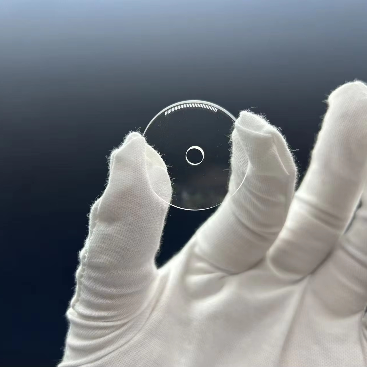
Frosted Quartz Sheet
Micro-sandblasted or acid-etched surface finish. Ideal for uniform beam homogenization, thermal baffles, and plasma masking.
View Product SpecsSupplying Japanese semiconductor fabs, optical laboratories, and chemical processing facilities across Kanagawa Prefecture with micro-machined, high-purity (≥99.99% SiO₂) quartz glass solutions.
Micro-sandblasted or acid-etched surface finish. Ideal for uniform beam homogenization, thermal baffles, and plasma masking.
View Product Specs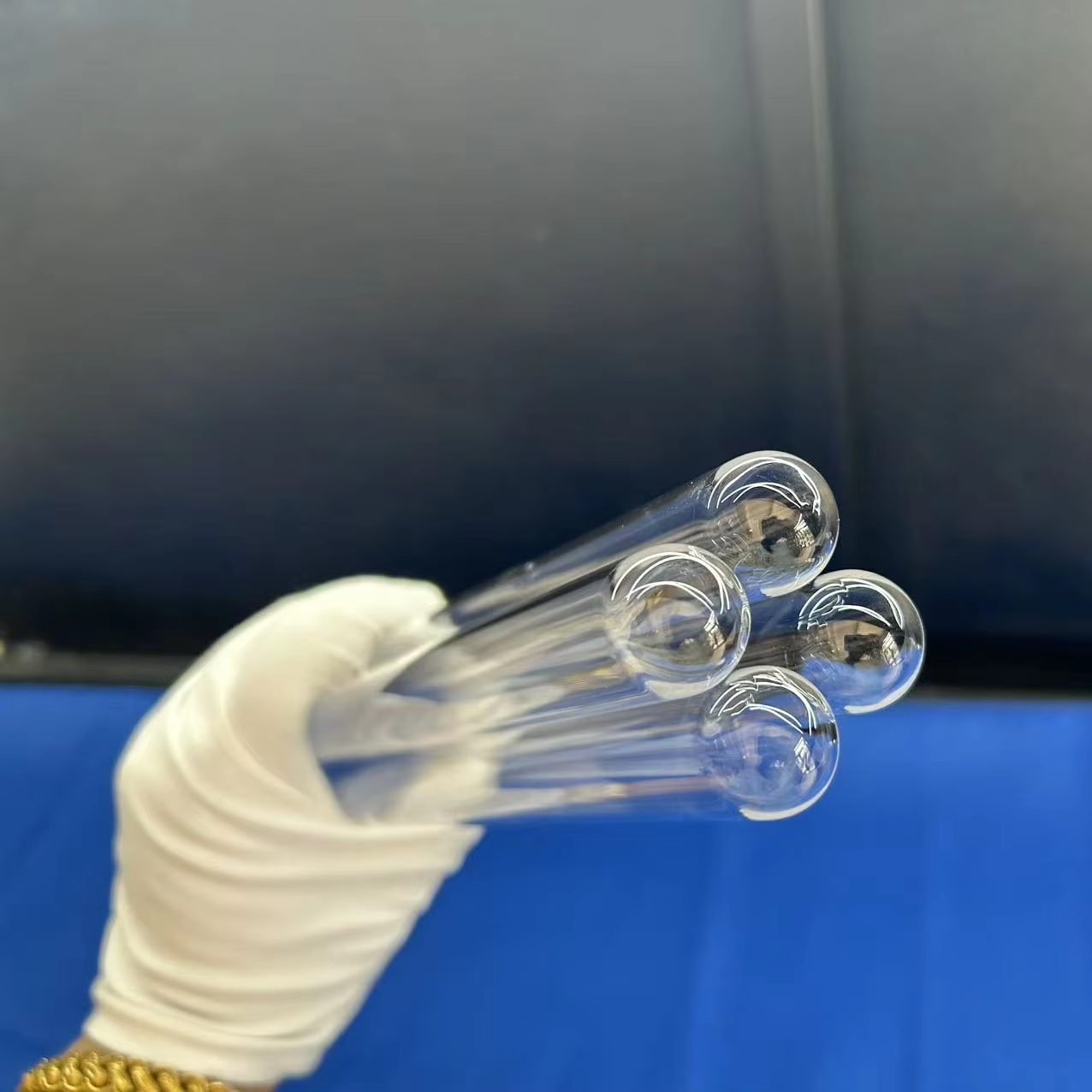
Precision sealed ends with custom flame-welding services. Engineered for pyrolysis, chemical synthesis, and inert sample collection.
View Product Specs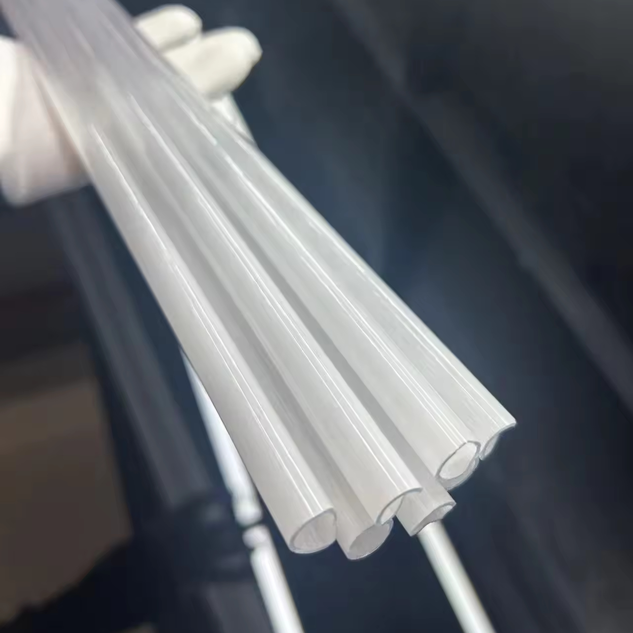
Thermal insulation sleeving with microporous opaque microstructure. Superb infrared reflectivity and thermal barrier efficiency.
View Product Specs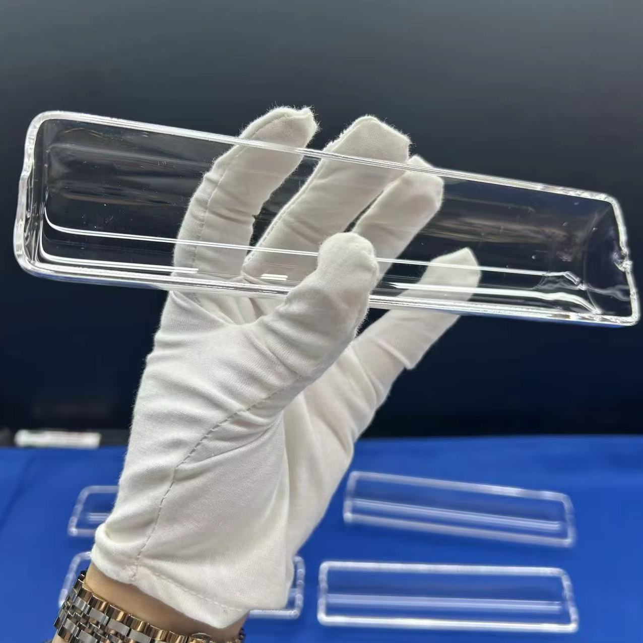
High-precision laser slotting for 2-inch to 12-inch silicon wafers. Annealed for high-temperature diffusion and wet chemical cleaning.
View Product Specs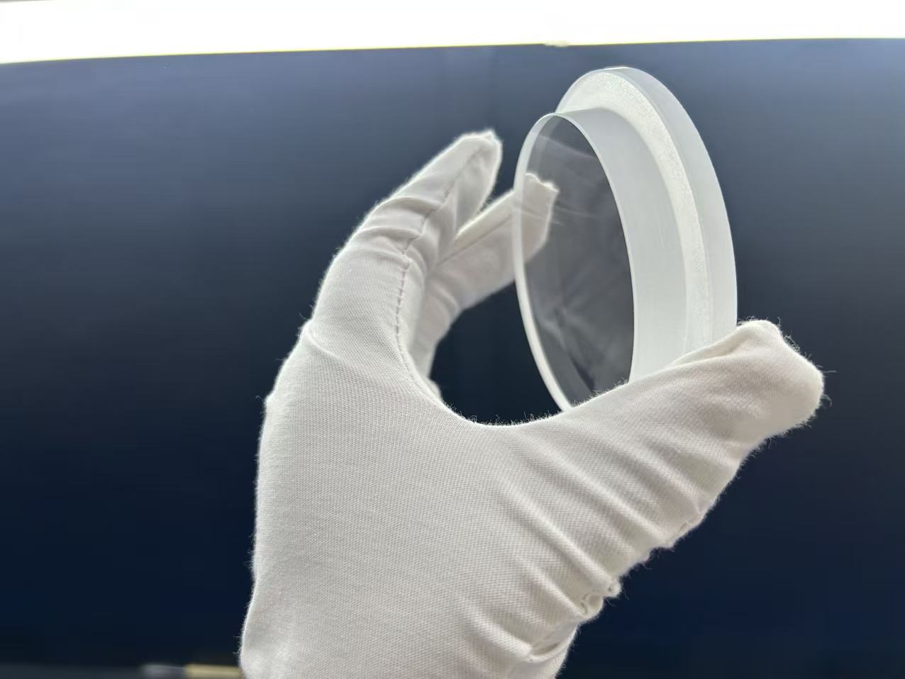
Tight dimensional tolerances (±0.02 mm) with step-lap CNC milling and fire-polished edges. Designed for chamber viewports and RF windows.
View Product Specs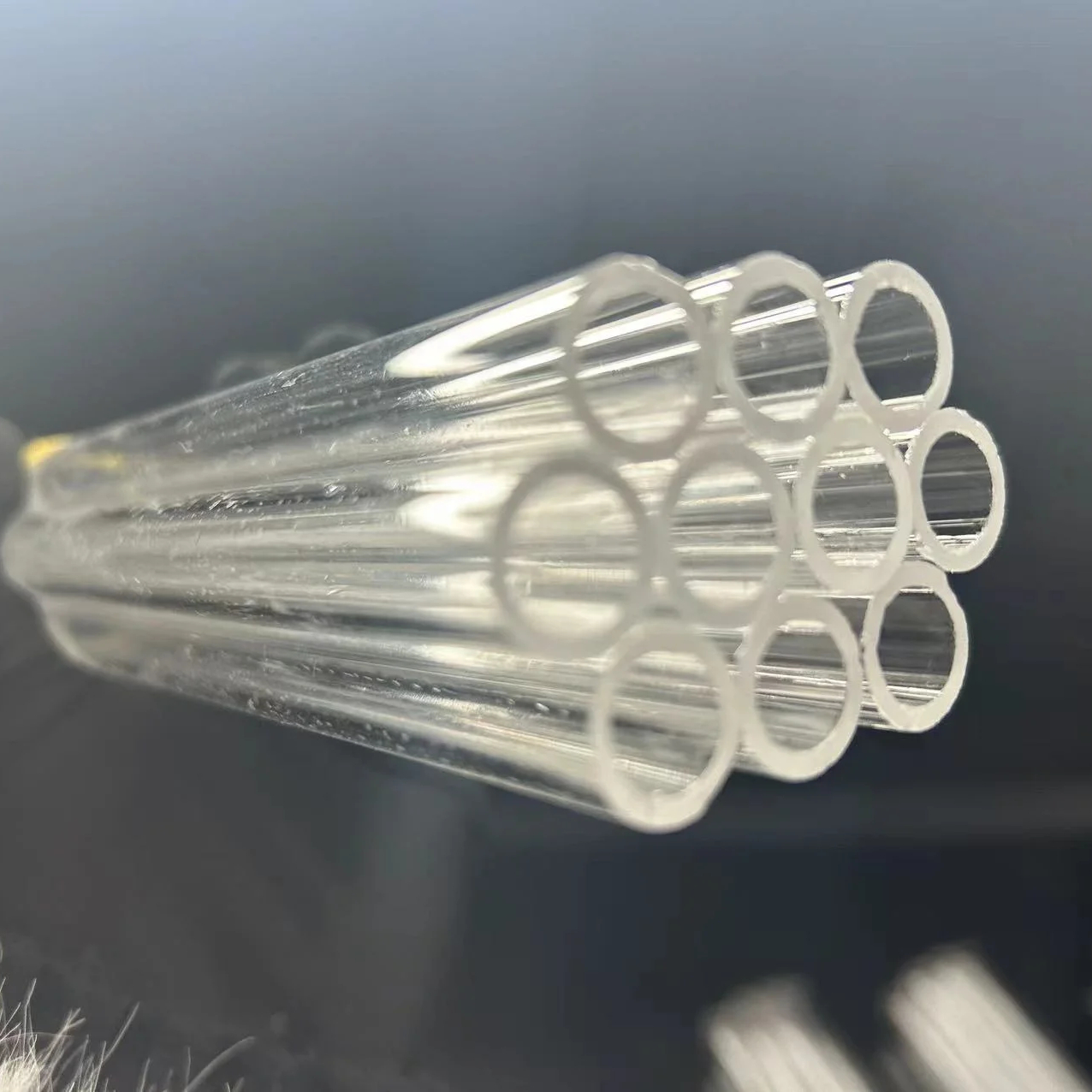
Bubble-free drawing with ultra-uniform wall thickness. Excellent thermal shock resilience from 1100°C down to rapid water quenching.
View Product Specs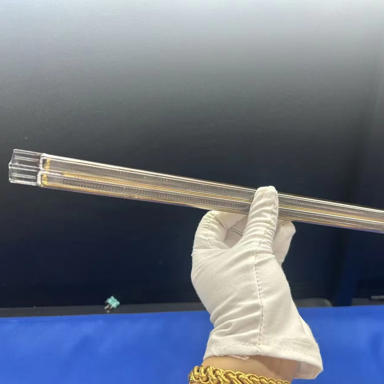
Next-generation infrared thermal radiation tube using carbon-graphene coatings for rapid thermal processing (RTP) and curing ovens.
View Product Specs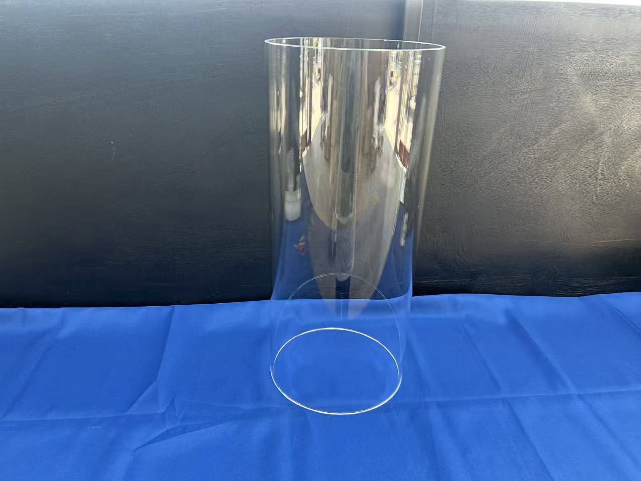
Outer diameters up to 450 mm with custom flange welding and optical end-plate bonding. Tailored for PECVD and LPCVD processing.
View Product SpecsIn high-precision manufacturing, microelectronics fabrication, and photonics research across Yokohama and the Kanagawa industrial corridor, the selection of transparent substrate materials demands uncompromising chemical purity, thermal stability, and optical homogeneity. Fused quartz discs—manufactured by melting high-purity natural crystalline quartz (SiO₂) or by chemical synthesis through silicon tetrachloride (SiCl₄) vapor oxidation (synthetic fused silica)—represent an essential class of amorphous engineering ceramics.
Unlike standard borosilicate or soda-lime glass, fused silica possesses an exceptionally rigid, three-dimensional tetrahedral lattice of silicon-oxygen bonds with no long-range crystalline order. This atomic arrangement produces an extraordinary coefficient of thermal expansion ($\alpha \approx 5.5 \times 10^{-7}\ \text{K}^{-1}$ between 20°C and 300°C), making quartz discs immune to thermal shock that would shatter conventional optical glasses. Yokohama engineering teams deploying viewports, vacuum sight glasses, and photolithography test substrates in plasma environments rely on this stability to maintain structural integrity under extreme thermal gradients.
| Optical Grade | Transmission Window | Hydroxyl (OH⁻) Content | Typical Ingot Synthesis Route | Primary Yokohama Applications |
|---|---|---|---|---|
| JGS1 (Synthetic Fused Silica) | 185 nm – 2500 nm (Deep UV) | < 1200 ppm (High OH) or < 50 ppm | Vapor phase axial deposition / Chemical flame hydrolysis | Excimer laser windows (193 nm / 248 nm), DUV lithography masks, UV spectrophotometry cuvette windows. |
| JGS2 (Optical Grade Quartz) | 220 nm – 2500 nm (UV-Vis) | < 30 ppm | Gas-oxygen flame fusion of purified crystal sand | Vacuum sight glasses, high-intensity discharge lamps, semiconductor inspection viewports in Keihin plants. |
| JGS3 (Infrared Fused Quartz) | 260 nm – 3500 nm (Near-to-Mid IR) | < 5 ppm (Water-free) | Vacuum electric melting / Plasma fusion | Infrared pyrometry viewports, thermal imaging substrates, CO₂ laser mirrors, heating furnace windows. |
Trace elemental impurities, particularly alkali metals (Na, K, Li) and transition metals (Fe, Cu, Ni, Cr), induce devitrification at elevated temperatures and form absorption bands that degrade ultraviolet transmission. Nivra Quartz enforces stringent spectral analysis via Inductively Coupled Plasma Mass Spectrometry (ICP-MS), maintaining total heavy metal content under 15 ppm for standard grades and under 1 ppm for semiconductor-grade synthetic discs. This purity profile ensures minimal mobile ion migration, making these substrates completely compatible with cleanroom processes operating at Class 100 or higher.
The transition from a raw fused quartz ingot into a laser-grade disc requires multi-stage abrasive machining, deterministic planetary double-sided lapping, and Chemical-Mechanical Polishing (CMP). At Nivra Quartz’s manufacturing base in Donghai County, high-purity quartz boules are first sliced using diamond multi-wire saws with micro-kerf tensioning, ensuring negligible subsurface micro-cracks and optimal material yield.
Subsequent core extraction and edge chamfering are conducted on high-speed 5-axis CNC machining centers. Edge treatment is critical for discs intended for Yokohama's vacuum and pressure vessels: a full radius (C-edge) or a 45-degree micro-chamfer is applied followed by optical flame-polishing or fine ground finish. This step eliminates edge micro-notches, raising the mechanical Weibull modulus and preventing mechanical failure under differential pressure in vacuum flanges.
Discs can be figured to $\lambda/4$ or $\lambda/10$ @ 632.8 nm over 90% clear aperture, verified via Zygo phase-shifting laser interferometers to avoid optical distortion in beam paths.
Controlled polishing regimens using colloidal silica slurries yield surface quality levels from commercial 60-40 down to laser-grade 20-10 and 10-5 for extreme laser fluence resistance.
Planetary double-sided lapping maintains parallelism under 10 arcseconds and TTV below 2 microns across wafers up to 300 mm in diameter, preventing wafer chuck clamping errors.
Yokohama is not only Japan’s premier trade gateway but also a powerhouse of advanced R&D, chemical engineering, and next-generation optical technology.
Along the coastal waterfront of Tsurumi-ku and Kanagawa-ku, petrochemical pilot plants and specialty gas synthesis lines utilize thick-wall fused quartz discs as explosion-proof sight glasses and UV degradation reaction windows, enduring temperatures above 1000°C alongside corrosive chlorine and sulfur dioxide vapors.
The cluster of semiconductor toolmakers and metrology developers in Kohoku New Town requires ultra-flat JGS1 synthetic quartz circular discs for wafer transfer chuck testbeds, optical alignment calibrators, and vacuum chamber viewport windows, guaranteeing unhindered laser transmission at 266 nm and 355 nm wavelengths.
From photonics-electronics convergence (IOWN) labs in Minato Mirai to biomedical researchers at RIKEN Center for Integrative Medical Sciences (Yokohama Campus), high-transmittance JGS1 quartz discs are specified as microfluidic cover plates, deep-UV fluorescence windows, and quantum diamond-NV center test substrates.
Navigating the strategic transformations shaping Kanagawa Prefecture's advanced procurement requirements.
As 2.5D and 3D chiplet architectures push organic interposers to their thermal and mechanical limits, semiconductor R&D in Kanagawa is accelerating transitions toward fused silica wafer cores. Fused quartz discs with coefficient of thermal expansion closely matching silicon offer superior rigidity, low RF dielectric loss at high frequencies (>40 GHz), and extreme planarity for next-generation AI processors.
With Yokohama Port targeted as a national demonstration hub for liquid hydrogen and ammonia combustion, industrial testing facilities demand specialized observation windows. Fused quartz discs with zero OH content (JGS3) are increasingly deployed in high-pressure combustion chambers, resisting severe thermal shock and water-vapor-induced devitrification during continuous 1100°C operations.
Japanese procurement leaders are actively mitigating sole-source exposure by qualifying high-capacity Chinese manufacturing partners capable of meeting strict Japanese Industrial Standards (JIS). Nivra Quartz provides an optimal dual-sourcing bridge: direct access to raw crystal resources in Donghai combined with transparent metrology data, reducing component lead times by up to 45% compared to domestic Japanese job shops.
Detailed answers addressing dimensional tolerances, customs documentation, cleanroom packaging, and Japanese metrology expectations.
Our fused quartz and synthetic silica discs are manufactured and inspected in strict accordance with JIS R 3201 (Flat Glass testing methodologies) and JIS R 3257 (Substrate flatness by optical interferometry). Every export batch destined for Japan undergoes full dimensional verification (diameter, thickness, concentricity, bevel angle) and surface quality inspections. We provide comprehensive mill test certificates (MTC), laser interferometer interferograms, and spectrophotometer transmission traces (190 nm to 3200 nm) with each shipment.
The choice depends directly on the optical wavelength and operating temperature of your process:
• JGS1 (Synthetic Silica): Best for UV lithography, laser machining (248 nm, 266 nm, 355 nm), or deep-UV spectroscopic observation. It has practically zero bubble inclusion (Class 0 per DIN 58927) and high radiation resistance.
• JGS2 (Optical Quartz): The industry benchmark for standard semiconductor plasma chamber sight glasses, vacuum viewports, and lamp envelopes across the 260 nm – 2000 nm band. Highly cost-effective for visible-spectrum observation.
• JGS3 (Infrared Grade): Selected when process monitoring relies on IR pyrometers, thermal imaging cameras, or CO₂ laser transmission up to 3.5 μm, thanks to its water-free structure ([OH] < 5 ppm) eliminating the 2.73 μm hydroxyl absorption dip.
Our facility in Donghai County (Lianyungang, Jiangsu) enjoys direct connectivity to major maritime and air shipping routes. For expedited sample orders and low-volume pilot runs, door-to-door air freight to Tokyo Haneda (HND) or Narita (NRT) takes 3 to 5 business days, followed by rapid customs clearance into Yokohama. For bulk production shipments, containerized or LCL sea freight routes from Lianyungang or Qingdao Port directly to the Port of Yokohama (Honmoku or Daikoku Pier) typically take 7 to 10 days transit time.
We treat export packaging with the same precision as optical grinding. Finished quartz discs are ultrasonically cleaned, vacuum-sealed in static-dissipative Class 1000 cleanroom poly bags or individual polycarbonate wafer cassettes with dust-free interleaf paper. These are nestled within custom-molded high-density shock-absorbing EPE foam compartments inside inner cartons, and finally secured within export-grade, fumigation-free plywood crates reinforced with exterior metal banding and tilt/shock sensor indicators.
Yes. Our in-house machining workshop is equipped with multi-axis CNC ultrasonic milling, diamond drilling, and automated edge-profiling equipment. We accept 2D drawings (PDF, DWG, DXF) and 3D CAD files (STEP, IGES). Typical custom features include stepped flanges for O-ring sealing, blind counterbores, SEMI-standard orientation flats or alignment notches, laser serial number engraving, and through-holes as small as 0.5 mm diameter with crack-free chamfered edges.
We actively support R&D institutions, university spin-offs, and OEM engineering trials across Kanagawa Prefecture. For standard diameter discs (e.g., 2-inch, 4-inch, 6-inch, 8-inch, 12-inch or 50 mm to 300 mm), our MOQ starts from 1 to 5 pieces. Custom prototypes can be manufactured, measured, and dispatched within 7 to 12 working days upon drawing approval, enabling agile iteration for your development cycles.
Combining Donghai’s raw material supremacy with certified quality management, engineering responsiveness, and established global export capabilities.
Situated in China's quartz heartland, we possess direct vertical access to premium high-purity natural silica deposits and synthetic feedstock, insulating Yokohama buyers from raw material price volatility.
Founded in 2019, our workforce combines master glassblowers, CNC technicians, and metrology engineers dedicated to tight-tolerance optical quartz fabrication under certified ISO quality systems.
With an audited 88.89% inquiry response rate, our English- and Japanese-speaking technical support staff review your tolerances and supply complete DFM quotes within hours, never weeks.
Exporting over 40% of our capacity to Tier-1 buyers across North America, Europe, and Asia, our track record guarantees predictable quality, seamless customs compliance, and zero supply surprises.
Whether you require deep-UV JGS1 wafers for photolithography, heavy-wall JGS2 vacuum viewports for Keihin manufacturing plants, or custom-dimensioned fused silica plates, our application engineers are standing by to review your CAD files and technical specifications.