High-Purity Fused Quartz Components Ready for Bruges Sourcing
Directly shipped from our Donghai precision manufacturing base to West Flanders cleanrooms, university research hubs, and port industrial parks. Every part is certified to DIN/ISO 10110 optical standards.
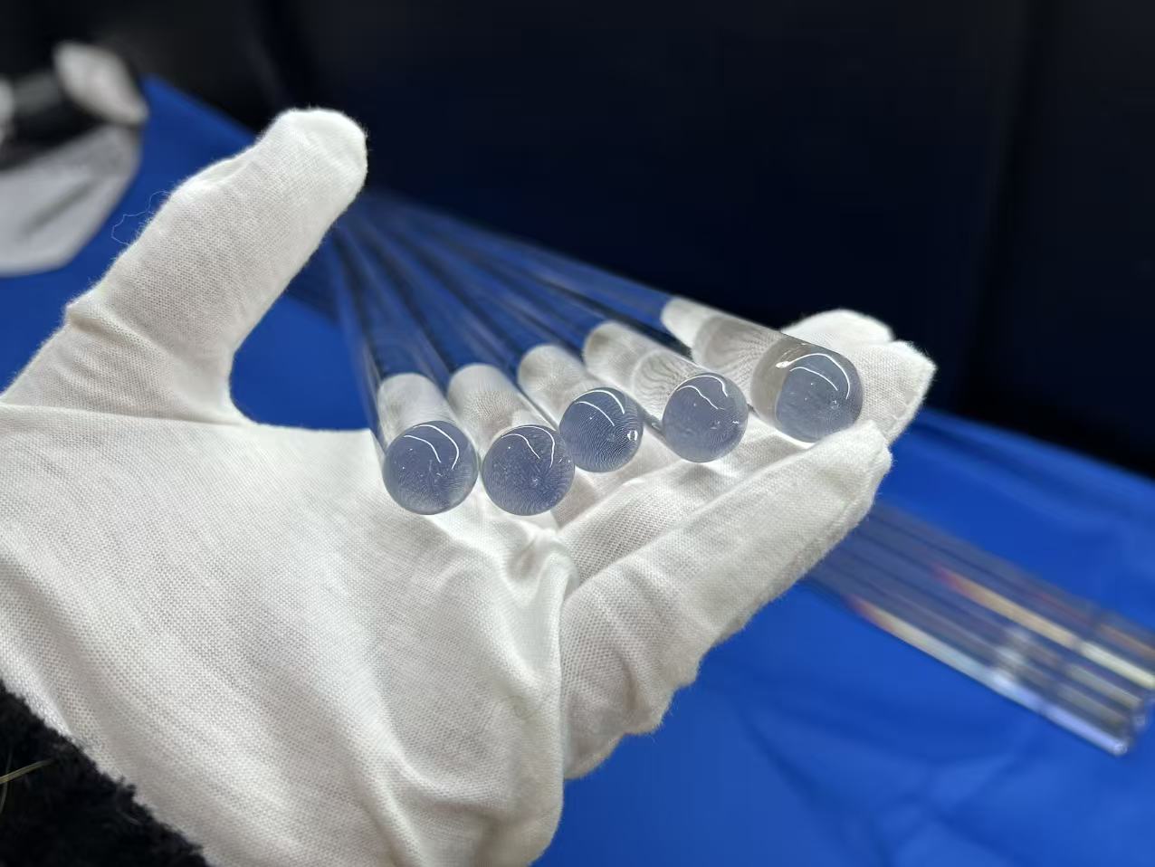
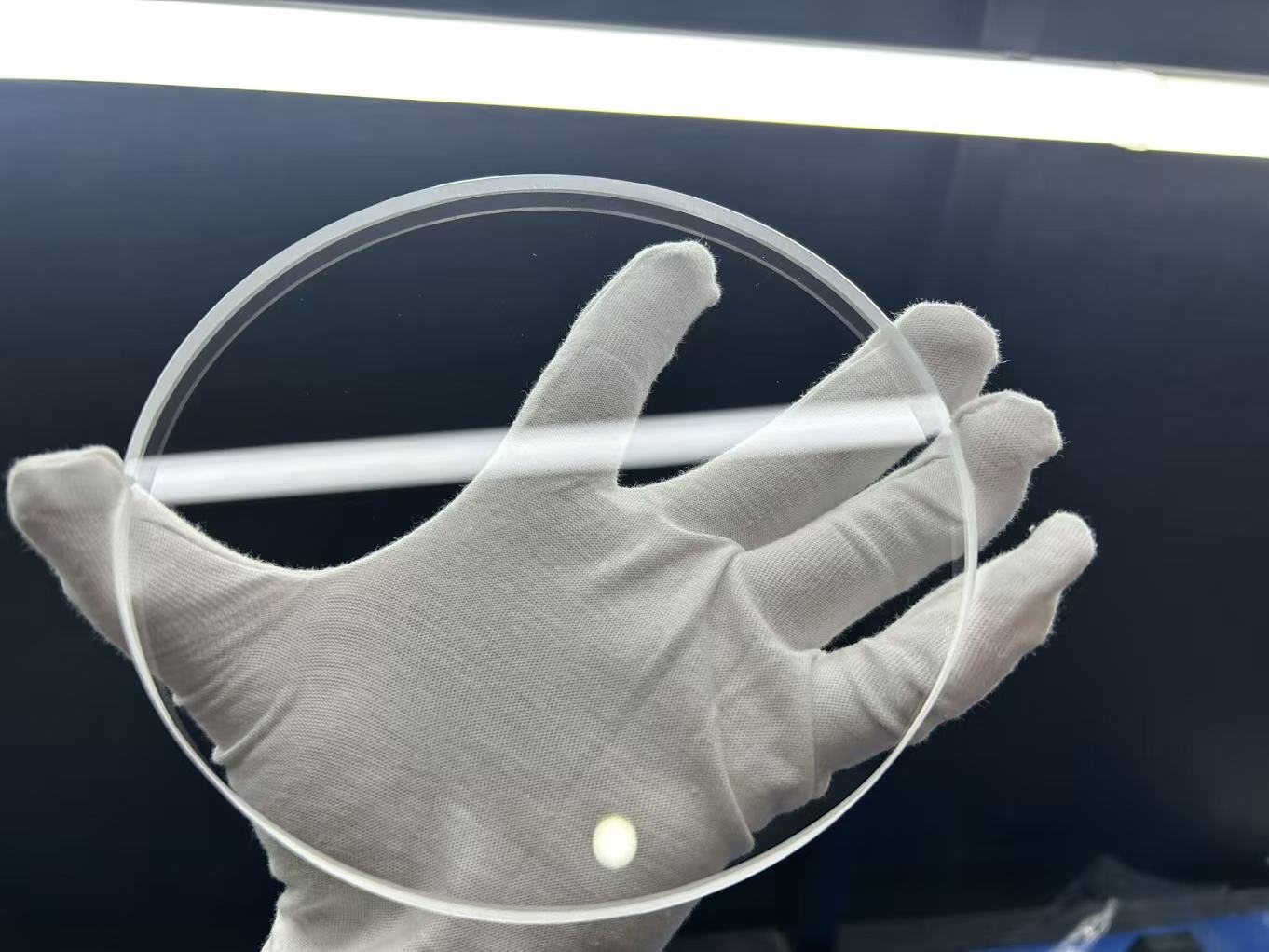
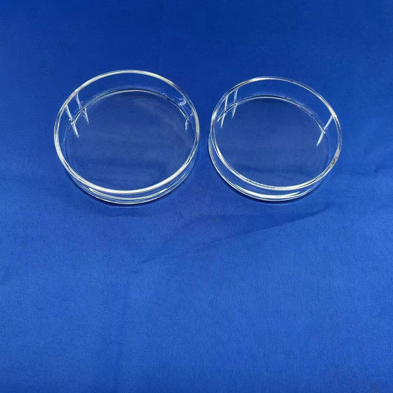
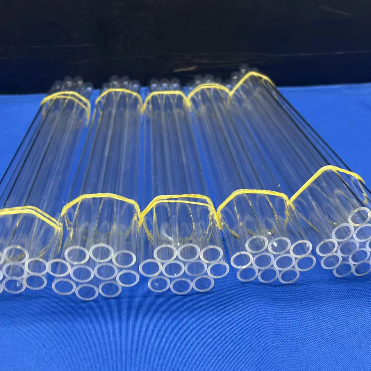
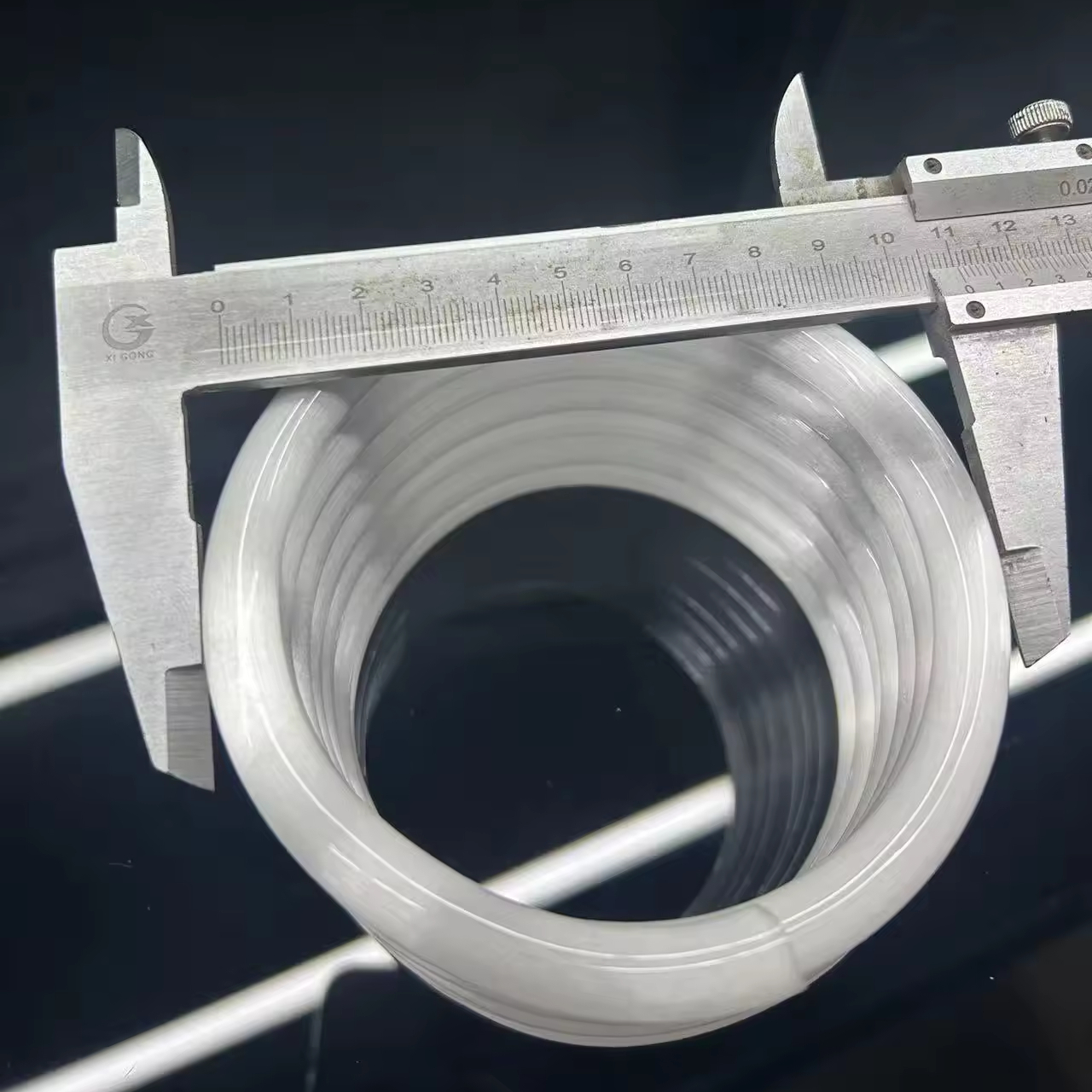
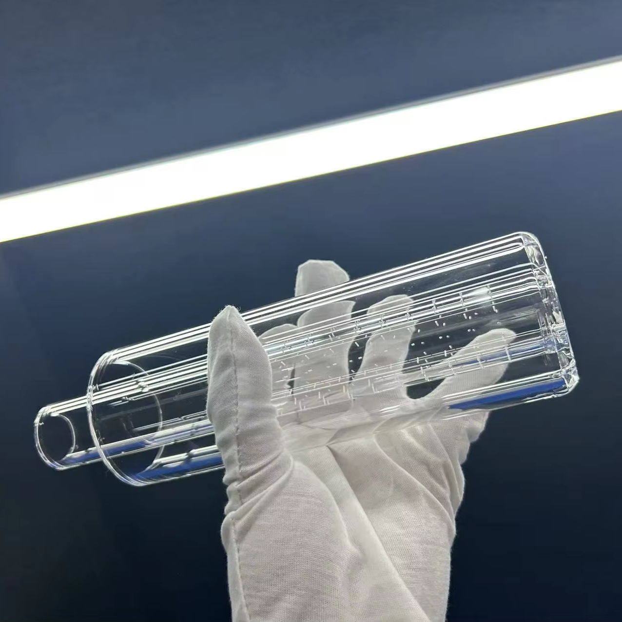
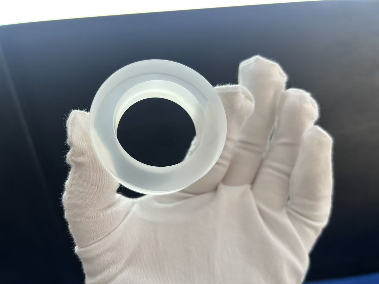
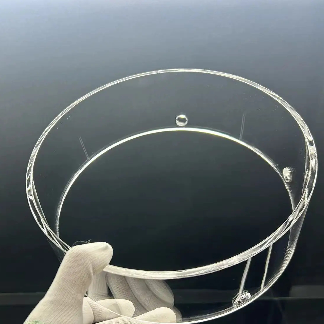
Engineering Metrology: Synthetic Fused Silica (JGS1) vs. Natural Fused Quartz (JGS2/JGS3)
For high-precision European applications, selecting the appropriate silicon dioxide ($SiO_2$) substrate requires an exhaustive understanding of deep-UV optical transmission, hydroxyl ($OH^-$) radical concentration, bubble classes, and thermal shock survivability. In the industrial ecosystem of Bruges and the wider Flanders region, precision instrumentation often fails due to microscopic inclusion densities or unwanted birefringence.
Nivra Quartz manufactures custom substrates under rigorous cleanroom conditions. Our synthetic grade JGS1 is produced via chemical vapor deposition of silicon tetrachloride ($SiCl_4$) precursors, yielding a material virtually free of metallic contaminants ($< 0.1\text{ ppm}$ total metals). This ensures extraordinary transmittance in the deep ultraviolet band down to $185\text{ nm}$, resisting excimer laser solarization at $193\text{ nm}$ and $248\text{ nm}$.
Conversely, our JGS2 optical grade utilizes refined natural crystal quartz from Donghai, delivering cost-effective transmission across the UV-visible-NIR spectrum ($220\text{ nm} - 2500\text{ nm}$). For infrared sensors and pyrometry applications, JGS3 is electrically vacuum fused to strip hydroxyl radicals ($OH < 5\text{ ppm}$), effectively eliminating the notorious absorption dip at $2.73\ \mu\text{m}$.
| Physical Property | JGS1 (Synthetic UV) | JGS2 (Optical Vis) | JGS3 (Low-OH IR) |
|---|---|---|---|
| Transmission Range | 185 - 2500 nm | 220 - 2500 nm | 260 - 3500 nm |
| Hydroxyl ($OH^-$) Content | 1200 - 1500 ppm | 150 - 200 ppm | < 5 ppm |
| Coefficient of Thermal Exp. | 0.54 × 10⁻⁶ /°C | 0.55 × 10⁻⁶ /°C | 0.55 × 10⁻⁶ /°C |
| Softening Point | 1730 °C | 1683 °C | 1680 °C |
| Refractive Index ($n_d$, 589.3nm) | 1.4585 | 1.4584 | 1.4584 |
| Density ($\text{g/cm}^3$) | 2.20 | 2.20 | 2.20 |
| Bubble Class (DIN 3140) | Class 0 (Bubble-free) | Class 1 | Class 1 |
| Dielectric Constant (1 MHz) | 3.75 | 3.78 | 3.78 |
Precision Quartz Substrate Engineering for the Bruges Economy
From maritime instrumentation at Port of Antwerp-Bruges (Zeebrugge) to biomedical research laboratories in West Flanders, our components fulfill specific local operational demands.
Maritime & Offshore LiDAR
Zeebrugge’s critical role in North Sea offshore wind infrastructure requires optical quartz windows resistant to saline corrosion, high hydrostatic pressure, and broad thermal swings (-20°C to +50°C).
Biomedical Analysis & Microfluidics
Supporting clinical testing clusters in Bruges and Ghent with ultra-flat fused quartz substrates, electrophoresis plates, and UV-transparent cuvettes with zero background autofluorescence.
Laser & Optoelectronic Systems
High damage threshold fused silica windows (LIDT > 10 J/cm² at 1064nm, 10ns pulse) configured for industrial laser cutting, additive manufacturing heads, and fiber optic collimators across Flanders.
Green Hydrogen & Energy Pilot Cells
Zeebrugge’s green energy hub relies on high-temperature fused silica viewing flanges and electrochemical quartz cells for high-pressure electrolysis monitoring and solar thermal experiments up to 1100°C.
Technological & Sourcing Shifts in Flanders & Northwestern Europe
How Belgian research centers and OEM manufacturers are navigating European semiconductor supply chain diversification, tightening quality mandates, and sustainability standards.
Substrate Traceability & Contamination Budgets
As Belgian and Dutch photonics pilot lines scale up under European semiconductor initiatives, procurement engineers in the Bruges region are shifting from generic optical glass to rigorously certified, batch-traceable synthetic fused silica wafers. Metallic trace levels must adhere to strict ICP-MS certified parts-per-billion ceilings to prevent cross-contamination in vacuum deposition chambers.
Demand for Solarization-Resistant Substrates
With the expansion of UV-C disinfection devices, photochemical reactors, and high-harmonic laser systems, optical degradation has emerged as a primary failure point. Bruges industrial users increasingly mandate JGS1 synthetic silica featuring specific internal transmittance ($\tau \ge 90\%$ at 193 nm) to eliminate solarization-induced color center formation during prolonged UV bombardment.
Consolidated OEM Consumable Sourcing
Fluctuating European supply chains have prompted West Flanders firms to transition toward direct foundry OEM relationships. Rather than splitting procurement across multiple intermediaries, buyers consolidate quartz process tubes, wafer carrier boats, flanges, and optical inspection windows directly with Nivra Quartz to reduce total landed costs via Port of Antwerp-Bruges freight routes.
Why Bruges Procurement Teams Partner with Nivra Quartz
Based in Donghai County—China's crystal capital—with 101–200 skilled specialists, delivering certified direct-from-foundry quartz solutions backed by verifiable quality metrics.
Direct Source Value
Local mineral refining in Donghai guarantees unmatched cost advantages on 99.99% raw fused quartz without compromising dimensional tolerances or purity.
5-Hour Rapid Feedback
With an 88.89% inquiry response rate, our quartz engineers review your technical drawings (CAD/STEP/PDF) and provide manufacturing feasibility analysis within 5 hours.
Verified Export Integrity
On-site audited facility by independent third parties, maintaining a 5.0/5 buyer rating and over US$40,000 in recent verified transactions with European optics buyers.
Complete Processing Chain
In-house CNC diamond milling, ultrasonic micro-hole drilling, double-sided optical CMP lapping, and precision lathe flame annealing to mitigate internal residual stresses.
Frequently Asked Questions for Bruges & European Engineers
Comprehensive engineering guidance addressing tolerances, thermal survivability, shipping protocols, and customs compliance for Belgian clients.
1 How do I select between JGS1, JGS2, and JGS3 for our Bruges application?
Selection depends entirely on your working wavelength and optical power. JGS1 is a synthetic grade engineered for deep-UV (185–2500 nm) excimer lasers, lithography, and high-power UV spectroscopy. JGS2 is refined optical natural quartz (220–2500 nm) ideal for observation windows, sight glasses, and solar simulators. JGS3 provides dry quartz with extremely low hydroxyl content (OH < 5 ppm), preventing absorption in the 2.7 μm region for infrared thermal sensors and CO₂ laser optics.
2 What are the standard dimensional tolerances and surface flatness capabilities?
For custom fused silica substrates and wafers, our CNC double-sided lapping systems achieve diameter tolerances down to ±0.02 mm and thickness tolerances down to ±0.01 mm. Optical flatness is routinely inspected to λ/10 to λ/20 per inch at 632.8 nm, with surface roughness Ra < 0.3 nm RMS and scratch-dig specifications of 20-10 or 10-5 upon request.
3 How are fragile quartz substrates protected for sea/air shipping to Belgium?
Every optical wafer and substrate is individually sealed in anti-static, cleanroom-grade PET cases or vacuum bags, then cradled within high-density expanded polyethylene (EPE) shock-dampening foam. Shipments dispatched to Bruges or Zeebrugge travel in reinforced multi-layer export cartons or fumigation-free ISPM-15 compliant plywood crates with moisture barriers and tilt indicators.
4 What thermal shock limits can your fused quartz components survive?
Fused quartz features an exceptionally low coefficient of thermal expansion (approx. 5.5 × 10⁻⁷ /°C from 20°C to 300°C), which is nearly 1/20th that of standard soda-lime glass. Substrates can safely endure sudden heating to 1100°C followed by immediate quenching in 20°C water without catastrophic fracture, making them ideal for rapid thermal processing (RTP) equipment.
5 Are your products fully compliant with European RoHS, REACH, and CE directives?
Yes. Because our components consist of ≥99.99% high-purity SiO₂ without lead, cadmium, mercury, or harmful plasticizers, all materials comply fully with EU RoHS Directive 2011/65/EU and EU REACH Regulation (EC 1907/2006). Full trace metal analysis reports and Certificates of Conformity (CoC) accompany each production lot.
6 Can we order low-volume prototypes before launching series production?
Absolutely. While standard wafers typically run in batches of 20 to 100 units, we actively support European universities, engineering consultancies, and pilot plants in Bruges with small-run custom prototyping (as low as 1 to 5 pieces) to validate dimensions, optical coatings, and chemical compatibility prior to full-scale fabrication.
Request an Engineering Review & Quotation Within 5 Hours
Send us your technical drawings (PDF, DWG, or STEP formats), required material purity (JGS1 / JGS2 / JGS3), and dimensional tolerances. Our senior engineering team in Donghai will provide an itemized quote, feasibility analysis, and DDP Bruges / Zeebrugge logistics plan.