Featured Optical Substrates, Fused Quartz & Precision Thermal Glassware
Engineered in Donghai County—the crystal and quartz capital of China—our components satisfy strict semi-standard tolerances (±0.005mm), optical scratch-dig specifications (MIL-PRF-13830B), and thermal shock parameters demanded by Philippine OSAT cleanrooms and laser fabrication plants.
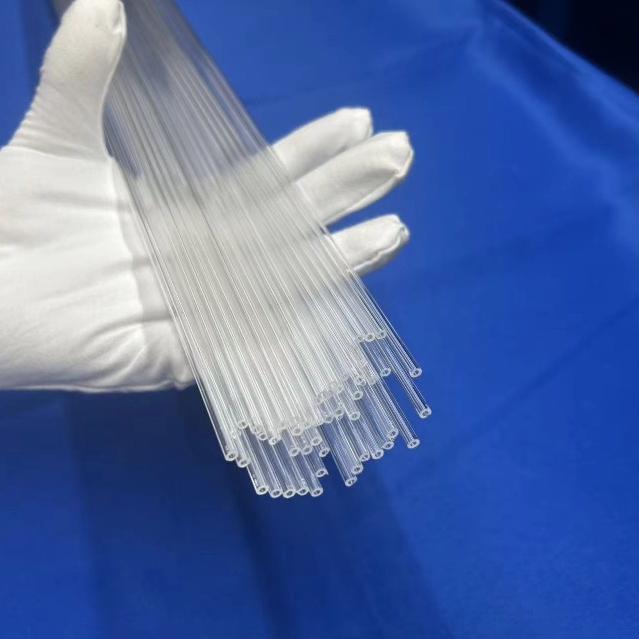
Capillary Quartz Tube
Precision micro-bore fused silica tubing designed for chromatography, fiber optic communication alignment sleeves, and analytical dosing equipment across Cavite electronics hubs.
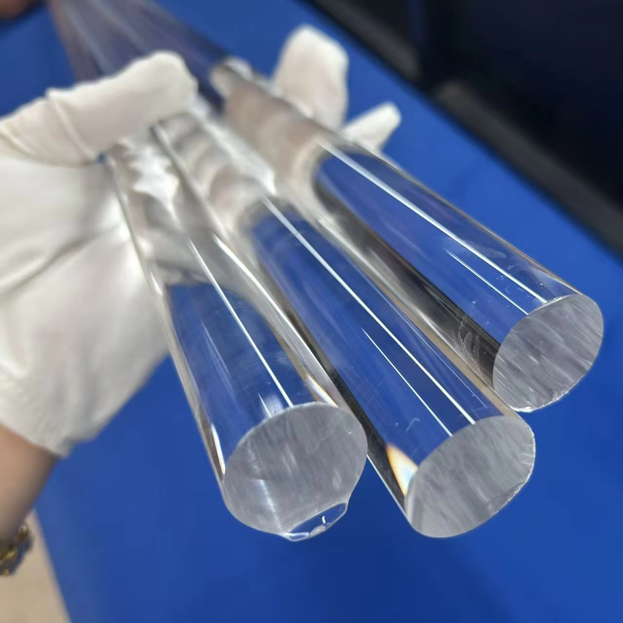
High-Purity Fused Quartz Large Diameter Round Rods
Custom cutting, diamond grinding, bending, and optical torch welding services for heavy-duty semiconductor furnace handles, structural supports, and fiber preforms.
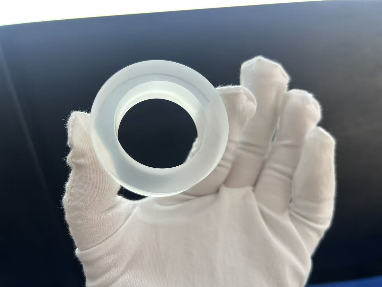
Precision Quartz Ring
High-temperature, chemical-resistant confinement and focus rings for plasma etching chambers, wafer clamping chucks, and epitaxial CVD reactors in Laguna Technoparks.
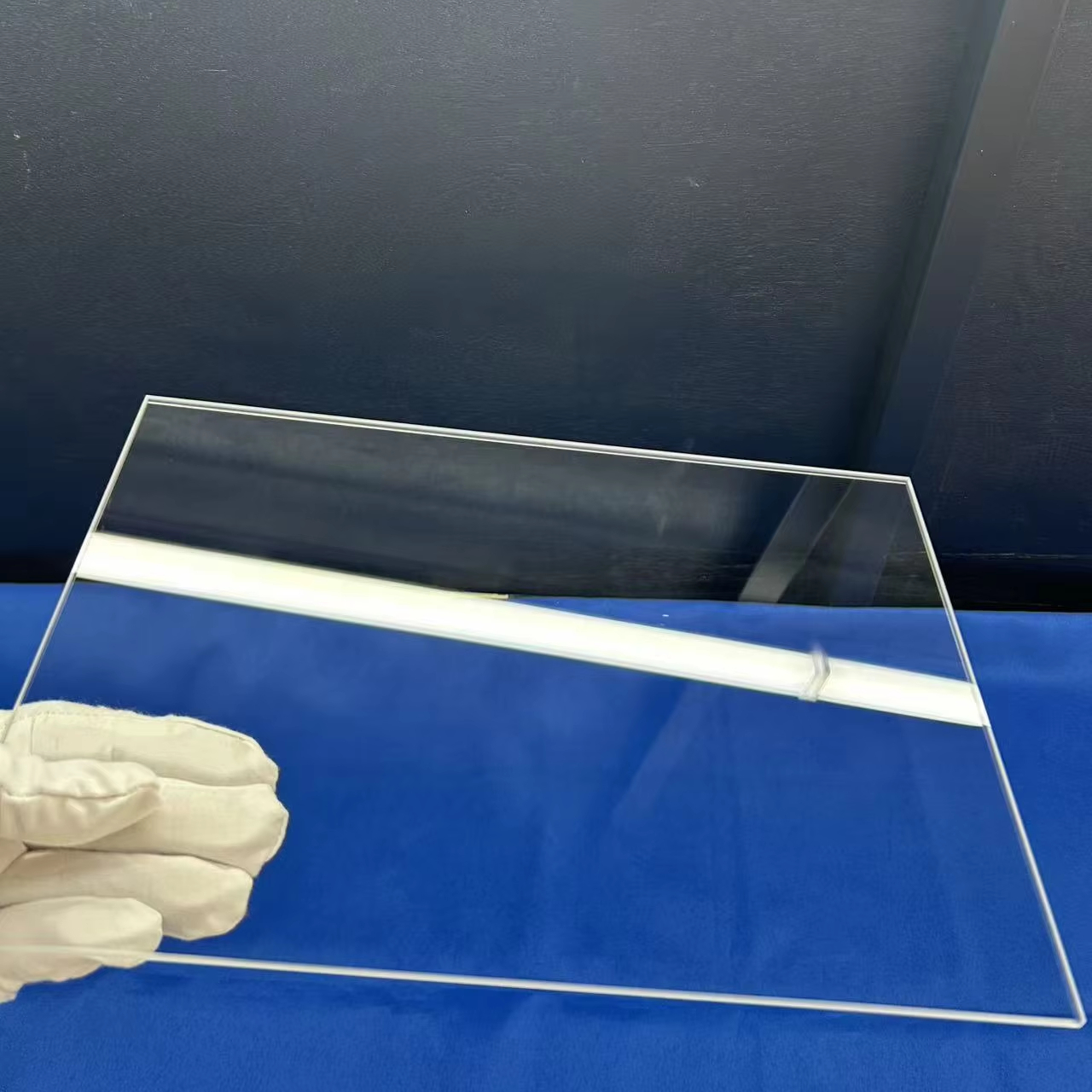
Custom Polished Square Quartz Glass Clear Plate 4mm
Double-side CMP polished optical windows featuring JGS1 synthetic grade deep UV transmission (>90% at 193nm) for lithography masks, sight glasses, and laser inspection devices.
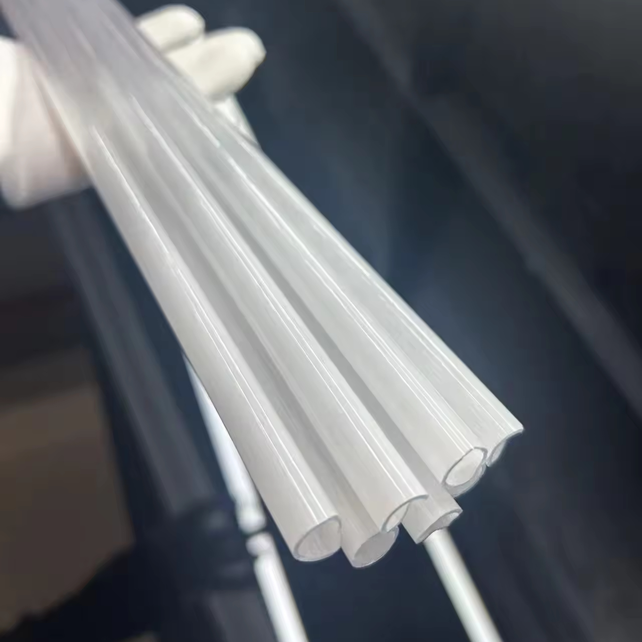
Translucent Milky White Quartz Glass Tube & Sleeve
Opaque fused silica thermal barriers offering superior infrared diffusion, thermal buffering, and electrical isolation up to 1150°C in industrial semiconductor annealing furnaces.
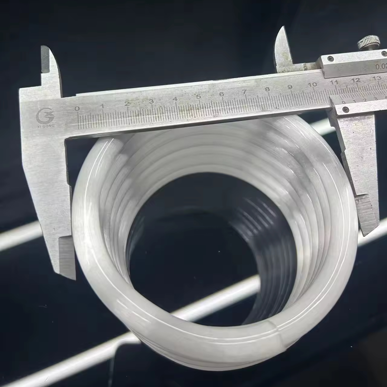
Helical Clear Quartz Glass Coil Tube
Thermal-shock-resistant spiral condensation coils and reaction tubes custom-coiled for chemical condensation, ICP cooling jackets, and high-purity acid recirculation.
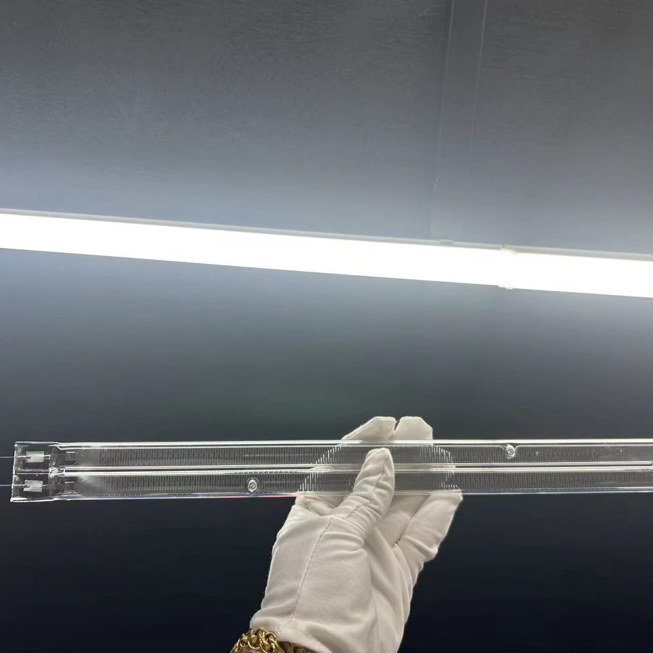
220V 700W Infrared Rapid Heating Quartz Tube
Carbon fiber and halogen medium-wave infrared heating tubes engineered for electronics reflow soldering, SMT curing lines, and solar photovoltaic wafer drying tunnels.
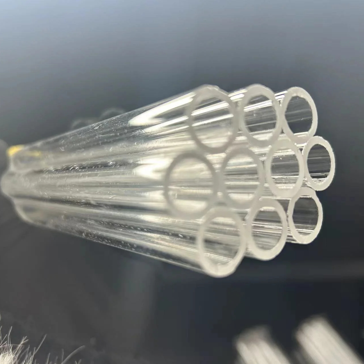
High Temperature Transparent Quartz Cylinder Tube
Flanged large-bore clear furnace process tubes engineered for silicon wafer oxidation, low-pressure CVD (LPCVD), and high-temperature diffusion operations up to 1450°C.
Material Engineering: Optical Sapphire Substrate vs. Synthetic Fused Quartz (JGS1/JGS2/JGS3)
Selecting between single-crystal sapphire (α-Al2O3) substrates and amorphous fused silica (SiO2) determines the operational longevity of optical sensors, UV-LED epitaxial layers, and semiconductor packaging components deployed in harsh tropical industrial environments.
Optical sapphire substrates manufactured via the Kyropoulos (KY) or Heat Exchanger Method (HEM) represent the pinnacle of mechanical hardness, dielectric integrity, and broadband optical transmission spanning 190 nm deep-ultraviolet to 5,000 nm mid-wave infrared. Single-crystal corundum structure imparts an extraordinary Mohs hardness of 9, making sapphire virtually immune to abrasive wear, particle scouring, and hydrofluoric acid vapor common in semiconductor dry-etching modules. Conversely, synthetic fused quartz (specifically Chinese standard grades JGS1, JGS2, and JGS3) offers zero birefringence, exceptional thermal shock resilience (quenchable from 1100°C to ambient water without catastrophic fracture), and ultra-low thermal expansion coefficients (≈ 5.5 × 10⁻⁷ /°C).
For Philippine manufacturing organizations operating under PEZA (Philippine Economic Zone Authority) regulations in Calabarzon, Clark, and Subic, balancing the higher thermal conductivity of sapphire (35 W/m·K at 25°C) against the cost-effective scalability of large-diameter fused quartz plates is paramount for optimizing capital equipment budgets.
| Crystalline / Material Property | Monocrystalline Sapphire (α-Al2O3) | Synthetic Fused Silica (JGS1) | Optical Fused Quartz (JGS2) | Infrared Fused Quartz (JGS3) |
|---|---|---|---|---|
| Crystallographic Structure | Hexagonal / Trigonal (Single Crystal) | Amorphous SiO2 (Synthetic) | Amorphous SiO2 (Natural Fused) | Amorphous SiO2 (Low-OH Fused) |
| Primary Crystallographic Planes | C(0001), R(1-102), A(11-20), M(10-10) | Isotropic (Non-crystalline) | Isotropic (Non-crystalline) | Isotropic (Non-crystalline) |
| Transmission Range (τ ≥ 80%) | 200 nm – 4,500 nm (Broadband) | 185 nm – 2,500 nm (Deep UV-VIS) | 220 nm – 2,500 nm (UV-VIS) | 260 nm – 3,500 nm (VIS to Mid-IR) |
| Mohs Hardness / Knoop Hardness | Mohs 9 / ~2000 kg/mm2 | Mohs 5.5 - 6.5 / ~460 kg/mm2 | Mohs 5.5 - 6.5 / ~460 kg/mm2 | Mohs 5.5 - 6.5 / ~460 kg/mm2 |
| Thermal Conductivity (25°C) | 35 – 40 W/(m·K) (Parallel to C) | 1.38 W/(m·K) | 1.40 W/(m·K) | 1.40 W/(m·K) |
| Coefficient of Thermal Expansion (CTE) | 5.8 × 10⁻⁶ /°C (Parallel) | 0.54 × 10⁻⁶ /°C | 0.55 × 10⁻⁶ /°C | 0.55 × 10⁻⁶ /°C |
| Hydroxyl (OH-) Concentration | < 1 ppm (Anhydrous Crystal) | ≈ 1,200 ppm (High Purity) | ≈ 150 – 200 ppm | ≤ 5 ppm (Water-Free IR Band) |
| Surface Roughness (CMP Finish) | Ra ≤ 0.2 nm (AFM Inspected) | Ra ≤ 0.3 nm – 0.5 nm | Ra ≤ 0.5 nm – 0.8 nm | Ra ≤ 0.5 nm – 0.8 nm |
| Primary Semiconductor Application | GaN/InGaN LED, SOS RFIC, SiC carrier | Excimer Laser Windows, UV Litho | Sight Glasses, CVD Process Tubes | Thermal Pyrometry, IR Gas Sensors |
Key Crystallographic Orientations for Philippine High-Tech Plants:
- C-Plane Sapphire (0001): Dominant substrate used by optoelectronic device manufacturers in Laguna Technopark for blue/green Gallium Nitride (GaN) epitaxial thin-film growth, high-brightness LEDs, and Micro-LED displays. Provides atomic-scale lattice matching and exceptional structural rigidity during high-temperature (1050°C) MOCVD processes.
- R-Plane Sapphire (1-102): Preferred for Silicon-on-Sapphire (SOS) CMOS semiconductor integrated circuits, high-frequency telecommunications switches, and rad-hard aerospace avionics components packaged within Baguio and Clark economic zones.
- A-Plane Sapphire (11-20): Delivers uniform dielectric constants and isotropic optical performance across the plane; widely chosen for electro-optical modulators, specialized pick-and-place end-effectors, and optical isolator substrates.
Target Application Scenarios Across Philippine Industrial Ecosystems
Serving multi-national semiconductor packaging (OSAT) conglomerates, consumer electronics manufacturing lines, and specialized marine optic facilities operating under PEZA jurisdiction.
Calabarzon Semiconductor & OSAT Hubs
Facilities across Cavite Economic Zone (CEZ), Light Industry & Science Park (LISP I-IV), and Laguna Technopark utilize our sapphire wafer carriers, CMP-polished dummy wafers, and quartz furnace boats for integrated circuit packaging, testing, and flip-chip underfill curing ovens.
Clark & Subic Aerospace Sensor Windows
Aviation instrument integrators and unmanned aerial systems (UAS) facilities in Clark Freeport Zone rely on our scratch-proof, pressure-resistant optical sapphire viewport discs and protective laser windows to resist particulate erosion and extreme atmospheric shear stresses.
Tropical Marine Optics & Subsea Systems
With an extensive coastline, Philippine naval sensing, offshore aquaculture telemetry, and deep-sea research stations require chemically inert optical domes. Fused quartz and optical sapphire withstand corrosive saltwater galvanic action and hydrostatic pressures up to 100 MPa.
DOST & Academic Precision R&D
Advanced prototyping laboratories at the Department of Science and Technology (DOST-MIRDC) and leading research universities (UP Diliman, DLSU) utilize custom fused quartz spectroscopic cuvettes, reaction tubes, and sapphire plates for chemical physics and nanotechnology research.
UV-C Disinfection & Industrial Photolysis
Water utility infrastructures and semiconductor ultrapure water (UPW) loop sanitization systems in Cebu and Metro Manila depend on high-transmittance JGS1 quartz immersion sleeves and sapphire UV sensor windows resistant to solarization and microbial fouling.
Philippine Electronics Industry Trends & Direct Sourcing Dynamics
Strategic alignment with the SEIPI (Semiconductor and Electronics Industries in the Philippines Foundation, Inc.) Roadmap and CREATE MORE Act fiscal modernization policies.
Shift Toward Advanced Heterogeneous Packaging
As the Philippine electronics export sector surpasses $45B annually, OSAT firms are transitioning from wire-bond packaging toward 2.5D/3D wafer-level chip-scale packaging (WLCSP). This transition surges local demand for high-planarity sapphire carrier substrates (TTV < 2 μm) and ultra-flat fused quartz handling discs capable of surviving high-vacuum thermal compression bonding.
PEZA Duty-Free Raw Material Corridors
Under Republic Act No. 11534 (CREATE Act) and PEZA regulations, registered manufacturing enterprises in Batangas, Laguna, and Cavite enjoy duty-free importation and value-added tax (VAT) zero-rating for critical optical consumables. Nivra Quartz provides certified non-VAT commercial documentation, standard dual-language packing lists, and Form E certification for zero-tariff clearance under ACFTA.
Resilient Short-Haul Maritime & Air Logistics
Mitigating cross-Pacific shipping bottlenecks, our direct transport corridor from Lianyungang / Shanghai Seaport delivers ocean container freight to Manila International Container Port (MICP) or Batangas Port within 5 to 7 days. Urgent wafer prototype runs are expedited through Clark International Airport (CRK) and NAIA via DHL/FedEx within 48 to 72 hours.
Engineered Precision: Factory Strengths in Donghai, Jiangsu
Donghai County Nivra Quartz Products Co., Ltd. combines geographic proximity to the world's premier quartz crystal reserves with state-of-the-art optical slicing, grinding, and CNC fire-working capabilities.
Direct From Crystal Capital
Sourcing directly from our Donghai facility eliminates middle-tier markups. We maintain 101–200 skilled operators executing diamond-wire slicing, CNC ultrasonic drilling, and computerized optical polishing in-house.
Rapid Technical Response
We respect tight packaging maintenance windows. Inquiries from Philippine engineers receive technical drawing reviews and pricing confirmations within ≤5 hours, backed by an audited 88.89% inquiry resolution rate.
Class 100/1000 Cleanroom Packaging
To eliminate particulate contamination during international transit across high-humidity sea routes, optical components are ultrasonic solvent-cleaned, vacuum-sealed in nitrogen-flushed anti-static bags, and cushioned in custom EPE molds.
Comprehensive Metrology COA
Every substrate batch is accompanied by Certificate of Analysis (COA) documentation, including Zygo laser interferometer surface flatness profiles, AFM roughness validation (Ra ≤ 0.2nm), and PerkinElmer UV-Vis-NIR spectrophotometer transmission curves.
Frequently Asked Questions for Philippine Procurement Teams
Addressing documentation, tariff structures, tropical climate considerations, and technical tolerance requirements for imports into the Philippines.
What specific documentation is provided for PEZA tax and tariff-exempt customs clearance?
For Philippine Economic Zone Authority (PEZA) registered locator enterprises in Cavite, Laguna, Batangas, and Clark, we provide complete sets of clean export documentation to ensure 0% VAT rating and import duty exemption under ACFTA (ASEAN-China Free Trade Area). This includes Form E (Certificate of Origin), commercial invoices stating the buyer's PEZA registration number, detailed packing lists with HS code classifications (HS 7104.99 for synthetic optical sapphire and HS 7020.00 for fused quartz industrial items), and airway bills directly consigned to your registered customs broker.
How does Nivra Quartz safeguard polished sapphire and quartz from tropical transit humidity?
The Philippines experiences sustained relative humidity levels exceeding 85% throughout the wet monsoon season. To prevent moisture condensation, chemical staining, and surface hazing on ultra-flat optical surfaces, all substrates undergo four-stage ultrasonic solvent cleaning, deionized water rinsing, and thermal vacuum baking. Each part is packed into cleanroom-certified wafer cassettes or individual polycarbonate carriers, vacuum-sealed inside multi-layer aluminum-foil moisture barrier bags (MBB) with active clay desiccants and calibrated humidity indicator cards before placement into shock-absorbent wooden export crates.
Can you manufacture non-standard sapphire substrates and custom quartz parts from CAD drawings?
Yes. Our core engineering strength lies in custom OEM/ODM manufacturing. We accept design files in STEP, IGES, DXF, DWG, and high-resolution PDF formats. We accommodate customized step-diameter discs, beveling, orientation flats (such as SEMI standard Primary and Secondary flats for wafer automated handling), CNC ultrasonic countersunk holes, and specialized laser engraving of lot tracing numbers on substrate edges.
What surface roughness (Ra) and flatness tolerances do your CMP-polished sapphire substrates achieve?
Our Chemical Mechanical Planarization (CMP) lines deliver semiconductor epi-ready finishes on both single-side polished (SSP) and double-side polished (DSP) substrates. Standard production achieves surface roughness Ra ≤ 0.2 nm (verified via Atomic Force Microscopy), Total Thickness Variation (TTV) < 3 μm (down to < 1.5 μm upon request), Bow < 5 μm, Warp < 5 μm, and surface optical quality conforming to 10-5 or 20-10 scratch-dig according to MIL-PRF-13830B.
What are the typical lead times and logistics routes from China to Philippine industrial parks?
Standard prototype samples and stocked tube/rod products ship within 3 to 5 business days. Custom CNC machining, lapping, and CMP polishing runs typically take 2 to 3 weeks depending on batch volume. Transit times via priority air cargo (CRK or NAIA airports) range between 48 to 72 hours. Consolidated Less-than-Container Load (LCL) or Full-Container Load (FCL) sea freight from Lianyungang or Shanghai port arrives at Manila South/North Harbor within 5 to 7 days, providing reliable procurement cycle predictability for continuous semiconductor assembly operations.
What is your Minimum Order Quantity (MOQ) for custom optical components?
We actively support engineering prototypes and pilot production runs. Standard quartz tubes, crucibles, and rods begin at an MOQ of 1 to 5 pieces. Precision polished sapphire discs, customized optical quartz plates, and micro-capillary tubes typically feature MOQs between 10 to 50 pieces, transitioning to scaled batch volume discounts for mass manufacturing agreements.