Export-Standard Fused Quartz & Silica Components
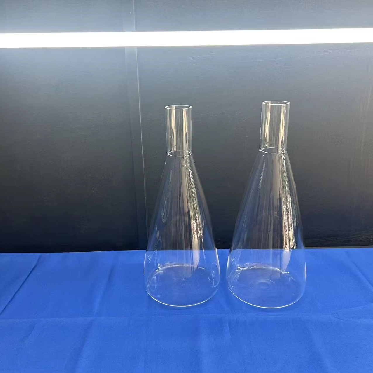
Direct factory production from Donghai County Nivra Quartz Products Co., Ltd. Ultra-high purity (SiO₂ ≥ 99.99%), precise dimensional tolerance, and bespoke CNC hot/cold processing.
Thailand's Advanced Manufacturing Nexus & The Sourcing Imperative
An engineering assessment of fused quartz substrate adoption throughout Bangkok, Samut Prakan, Pathum Thani, and the Eastern Economic Corridor (EEC).
The Kingdom of Thailand is rapidly pivoting toward high-complexity technology sectors under the national Thailand 4.0 framework. Long recognized as the automotive and hard disk drive (HDD) assembly center of Southeast Asia, Thailand's industrial belt—stretching from metropolitan Bangkok through the Eastern Economic Corridor (Chonburi, Rayong, and Chachoengsao)—is witnessing unprecedented capital deployment into outsourced semiconductor assembly and test (OSAT), compound semiconductor packaging (Silicon Carbide [SiC] and Gallium Nitride [GaN]), high-density interconnect (HDI) printed circuit board manufacturing, and Tier-1 photovoltaic (PV) cell production.
Critical to each of these high-temperature, chemically harsh manufacturing procedures is a foundational consumable: synthetic fused silica and natural fused quartz glass substrates. However, Southeast Asia lacks localized natural high-purity quartz reserves and thermal vitrification infrastructure. As an engineering consequence, industrial fabricators across Pathum Thani's high-tech industrial parks and Chonburi's free trade zones rely almost entirely on cross-border supply chains. China's quartz cluster, centered in Donghai County (Jiangsu Province), supplies over 80% of the world's commercial fused quartz material, serving as the strategic engine backing Thailand's advanced industrial roadmap.
For procurement directors, cleanroom operations managers, and thermal process engineers operating out of Greater Bangkok, quartz procurement presents significant technical friction. Sourcing generic borosilicate or lower-grade domestic commercial glass results in immediate structural catastrophic failure: devitrification at temperatures exceeding 500°C, thermal shock shattering under rapid quench cycling, trace transition metal outgassing that poisons semiconductor silicon wafers, and rapid micro-surface etching under hydrofluoric (HF) or phosphoric chemical cleaning cascades. Fused quartz substrates manufactured under rigorous ISO9001 precision standards at Donghai County Nivra Quartz Products Co., Ltd. bridge this performance gap, guaranteeing uncompromising chemical inertia, optical clarity, and mechanical stability.
Fused Silica vs. Natural Fused Quartz: Engineering Taxonomy
Selecting optimal optical and thermal grades (JGS1, JGS2, JGS3) to prevent over-specification overhead and operational down-time.
In precision manufacturing, "quartz" is not a monolithic material. The fundamental distinction lies between Synthetic Fused Silica—produced via chemical vapor deposition (CVD) or soot remelting of pure silicon tetrachloride ($SiCl_4$) precursors—and Natural Fused Quartz, synthesized by electrically fusing or oxy-hydrogen gas refining high-purity natural silica sand. Understanding the spectral transmission windows, trace metal inclusions (measured in parts per million, ppm), and hydroxyl ($OH^−$) ion concentration is critical for engineers in the Bangkok optical and electronics hub.
| Classification | Material Origin | Spectral Window | OH⁻ Content | Trace Impurity Total | Dominant Bangkok Applications |
|---|---|---|---|---|---|
| JGS1 Deep UV Grade | Synthetic Fused Silica (CVD) | 185 nm – 2,500 nm | < 1,200 ppm (standard) or < 50 ppm | < 0.1 ppm (Extremely Pure) | Excimer laser optics (193nm/248nm), DUV lithography masks, UV cuvettes, stepper windows. |
| JGS2 Optical Grade | Refined Natural Quartz Crystal | 220 nm – 2,500 nm | < 30 ppm | < 20 ppm | Optical sight glasses, high-intensity discharge (HID) lamp jackets, sensor substrates, inspection windows. |
| JGS3 Infrared Grade | Vacuum Electric Melted Silica | 260 nm – 3,500 nm | < 5 ppm (Water-free) | < 30 ppm | Thermal infrared emitters, CO₂ laser processing chambers, pyro-process observation ports, pyrometry. |
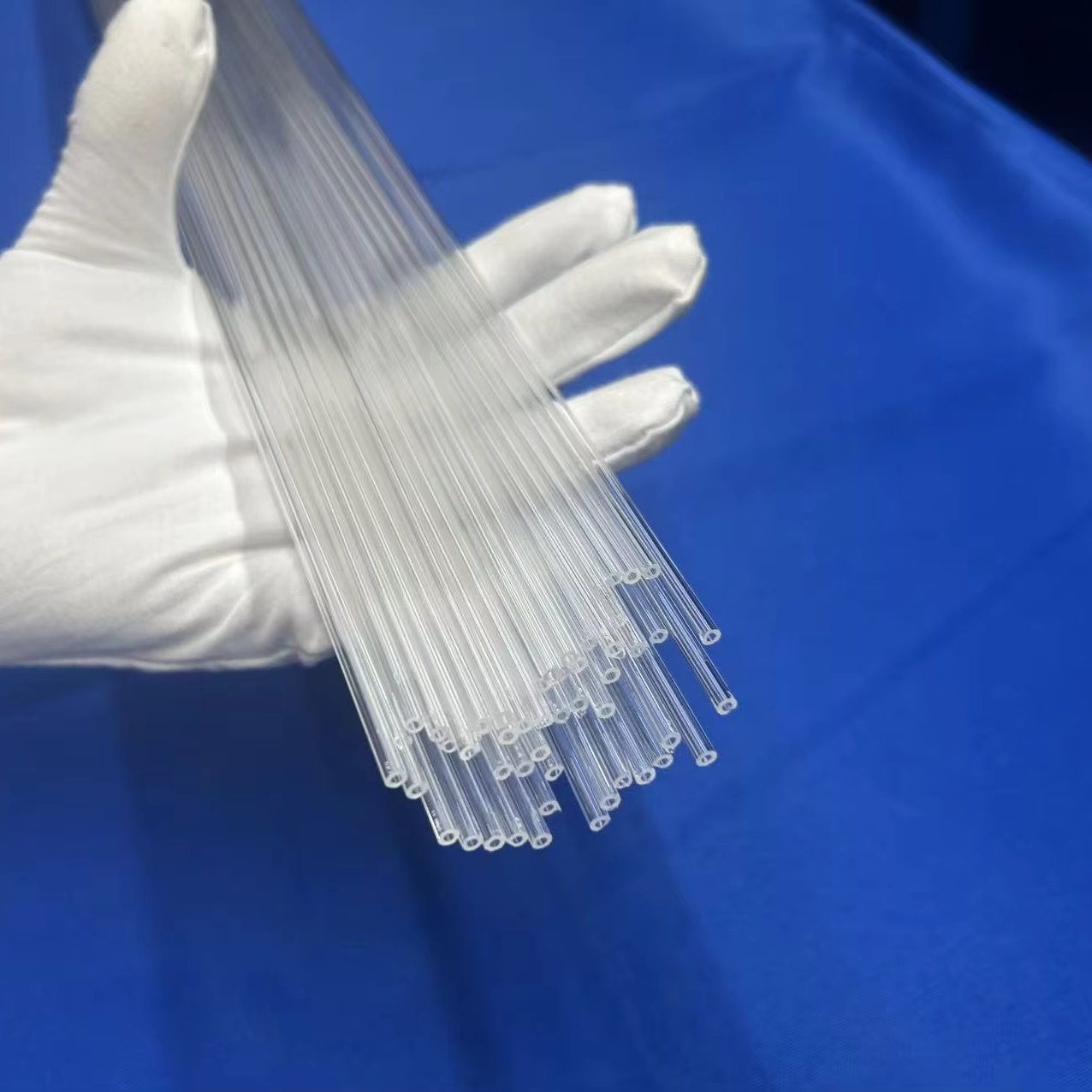
| Clear Fused Quartz | Continuous Fusion Tube/Rod | 300 nm – 2,500 nm | 15 – 30 ppm | < 50 ppm | Diffusion furnace tubes, wafer carrier boats, semiconductor cleanroom wet-etch tanks, thermocouple sheaths. |
| Monocrystalline Sapphire | Al₂O₃ Single Crystal | 190 nm – 5,000 nm | 0 ppm | Trace Cr, Ti, Fe | Scratch-resistant sensor covers, extreme high-pressure viewport glasses, aerospace avionics housings. |
Beyond transmission ranges, the thermo-mechanical tolerances of Nivra Quartz substrates solve chronic engineering problems in Thailand's ambient industrial climates. While soda-lime glass exhibits a high coefficient of thermal expansion ($\approx 90 \times 10^{-7}/\text{K}$) and borosilicate operates at $\approx 33 \times 10^{-7}/\text{K}$, Nivra clear fused quartz operates at an exceptionally low $5.5 \times 10^{-7}/\text{K}$. This allows a 100mm × 100mm × 3.0mm quartz substrate to be heated to 1100°C and plunged directly into 20°C ambient deionized water without experiencing micro-fracturing or catastrophic lattice cleavage.
Localized Application Scenarios in the Greater Bangkok Ecosystem
How leading manufacturing hubs in Thailand deploy Chinese fused quartz components to achieve precision, yield consistency, and thermal integrity.
Semiconductor OSAT & Wafer Handling
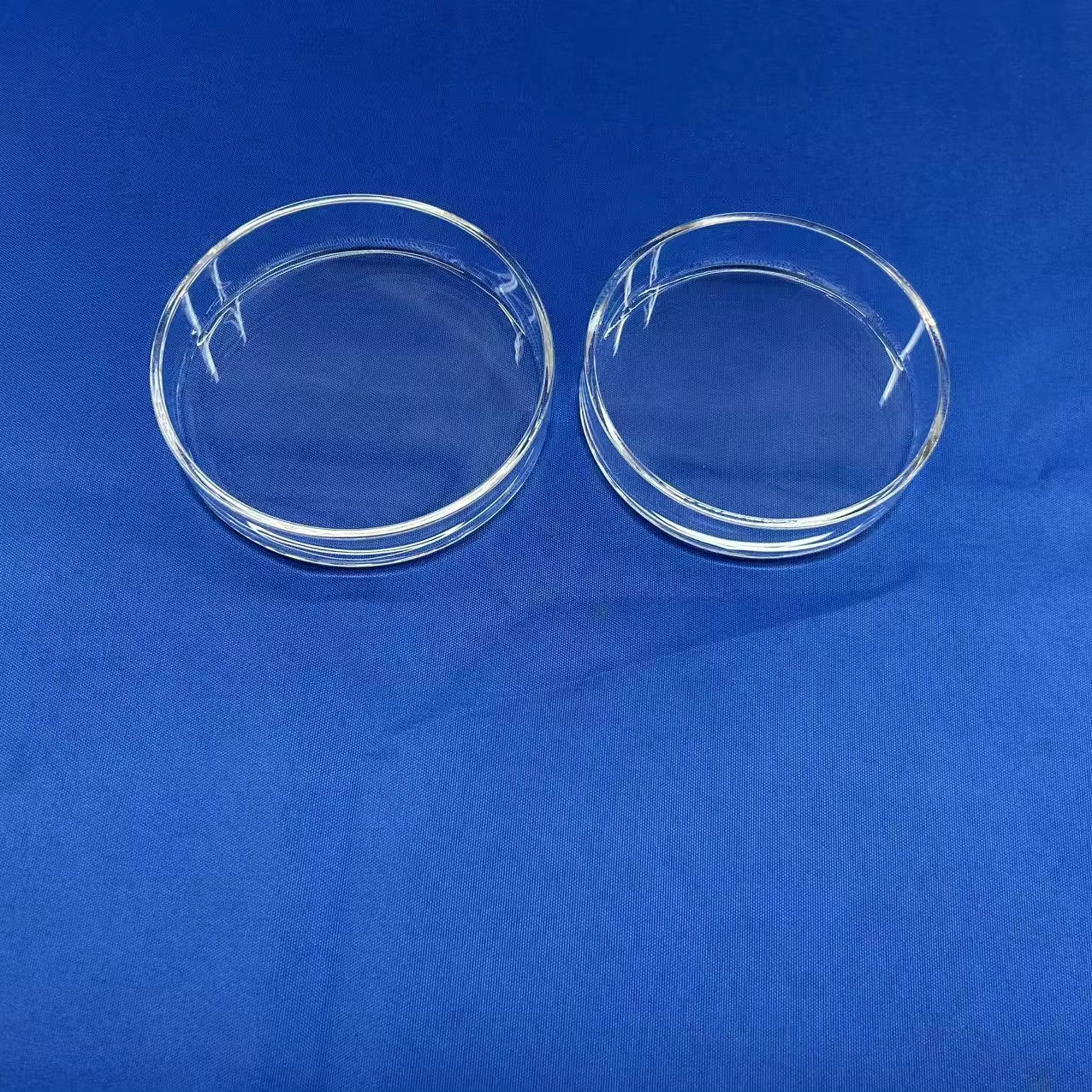
In the microelectronics hubs of Pathum Thani (Navanakorn Industrial Estate) and Bangkadi, packaging facilities utilize Nivra high-purity quartz carrier wafers and quartz boats. Quartz’s low dielectric loss, mechanical stiffness, and chemical resistance during aggressive acid wafer back-grinding and chemical mechanical planarization (CMP) ensure negligible wafer warp and zero heavy-metal ion contamination during packaging.
Solar PV Cell Fabrication (EEC Corridor)
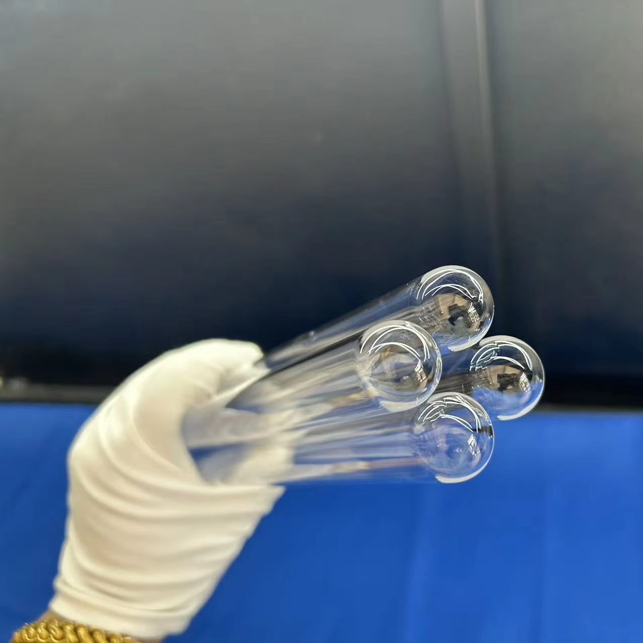
Rayong and Chonburi host global photovoltaic cell gigafactories. These facilities run multi-megawatt low-pressure chemical vapor deposition (LPCVD) and boron/phosphorus thermal diffusion tubes round the clock. Nivra produces large-diameter (OD 200mm – 450mm) high-purity fused quartz tubes with uniform wall geometry, resisting sagging and thermal devitrification at continuous 1150°C operational thresholds.
Rapid IR Curing for Automotive Assembly
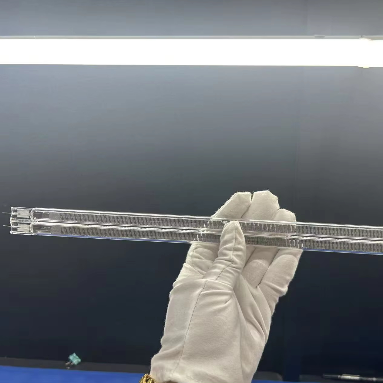
Samut Prakan, often called the "Detroit of Asia", houses automotive assembly lines utilizing high-speed infrared drying tunnels for paint, polymer resin, and battery cathode drying. Nivra’s carbon-fiber and halogen twin-tube quartz emitters provide high flux infrared density, instant on/off cycling, and precise wavelength control, drastically reducing energy draw compared to conventional convection ovens.
Academic & Clinical Spectroscopy Labs
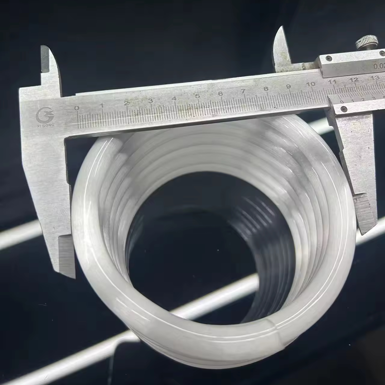
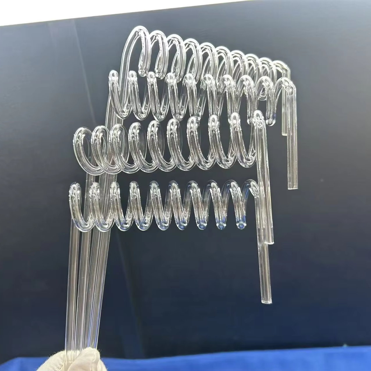
Institutions such as Chulalongkorn University, Mahidol University, KMUTT, and the Thailand Institute of Scientific and Technological Research (TISTR) rely on Nivra’s precision JGS1 UV spectrophotometer cuvettes, helical coil tubes, and custom glassware. Absolute optical symmetry, sub-micron path-length tolerances, and zero internal air-bubble inclusions ensure reproducible analytical data.
Industrial Laser & LiDAR Sensor Integration
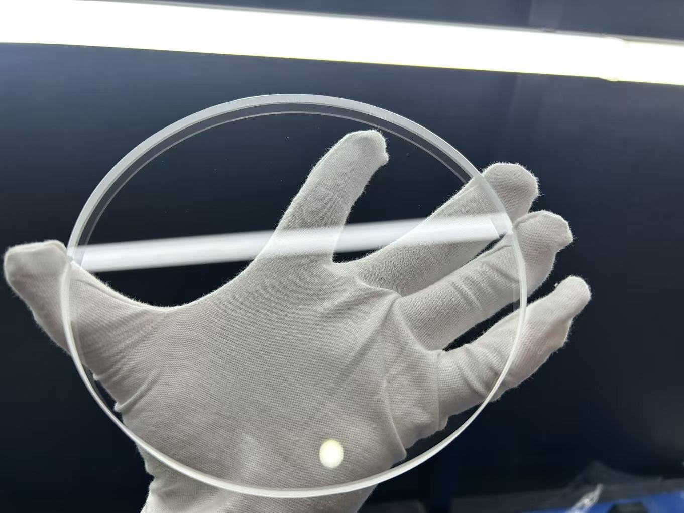
Advanced robotics developers in Lat Krabang leverage double-side polished JGS1/JGS2 synthetic fused silica plates as protective debris windows for fiber laser cutters (1064nm) and agricultural drone LiDAR sensors. The substrate's high laser damage threshold (LDT > 10 J/cm² at 1064nm, 10ns pulses) prevents thermal distortion, focal drift, and optical pitting in humid field environments.
Key Market Trends Shaping Quartz Substrate Consumption in Bangkok
Technological transformations, policy incentives, and supply chain shifts redefining industrial glassware procurement in Thailand.
1. OSAT & PCB Relocation to Thailand
Geopolitical diversification is accelerating multinational investments in PCB, substrate, and packaging foundries across Greater Bangkok. As Tier-1 manufacturers establish cutting, etching, and cleanroom lines in Thailand, local plant maintenance teams require direct, rapid delivery of standard and custom quartzware without relying on Western distributors' 16-week lead times.
2. Electric Vehicle (EV) Ecosystem Expansion
Backed by the Thailand Board of Investment (BOI) 30@30 policy, Bangkok has transformed into Southeast Asia’s epicenter for EV powertrain and lithium battery assembly. This surge has spiked demand for specialized infrared quartz heating banks and ultra-pure quartz electrolytic cleaning tanks used in high-voltage battery cell production and copper foil surface treatments.
3. Demand for Sub-Nanometer Surface Tolerances
As Thai optical sensor and camera-module manufacturers shift toward automated optical inspection (AOI) and autonomous machine vision, baseline surface requirements have migrated from commercial optical tolerances (60/40 scratch-dig) to laser-grade specifications: 20/10 or 10/5 scratch-dig, $\lambda/10$ transmitted wavefront distortion, and sub-nanometer surface roughness ($Ra < 0.2\text{ nm}$).
4. Form E & Belt-and-Road Nearshoring
With the upgrading of the ASEAN-China Free Trade Area (ACFTA), Thai importers benefit from 0% tariff preferential treatment under Certificate of Origin Form E. Coupled with established ocean freight routes connecting Shanghai/Lianyungang ports to Bangkok (Klong Toey) and Laem Chabang in under 8–10 days, direct sourcing from Chinese factories has become significantly more cost-efficient than regional intermediaries.
Donghai County Nivra Quartz: Factory Strengths & Infrastructure
Combining rich crystal regional heritage with modern 5-axis CNC machining, optical metrology, and global supply guarantees.
Founded in February 2019, Donghai County Nivra Quartz Products Co., Ltd. is headquartered at 285 Heping East Road, Donghai County, Lianyungang, Jiangsu Province—globally acknowledged as China's crystal and quartz capital. Spanning modern workshops staffed by 101 to 200 skilled glassblowers, CNC machinists, and optical inspection engineers, Nivra combines integrated mining-hub material access with cutting-edge manufacturing.
Our verified facilities have undergone comprehensive on-site audits by independent third-party inspection firms (including Alibaba.com field verification). From diamond cutting and deep-hole drilling to double-sided optical polishing, computerized flame lathe sealing, and stress-relieving annealing ovens, our end-to-end processing pipeline ensures every quartz tube, substrate wafer, and custom vessel complies with rigid design drawings.
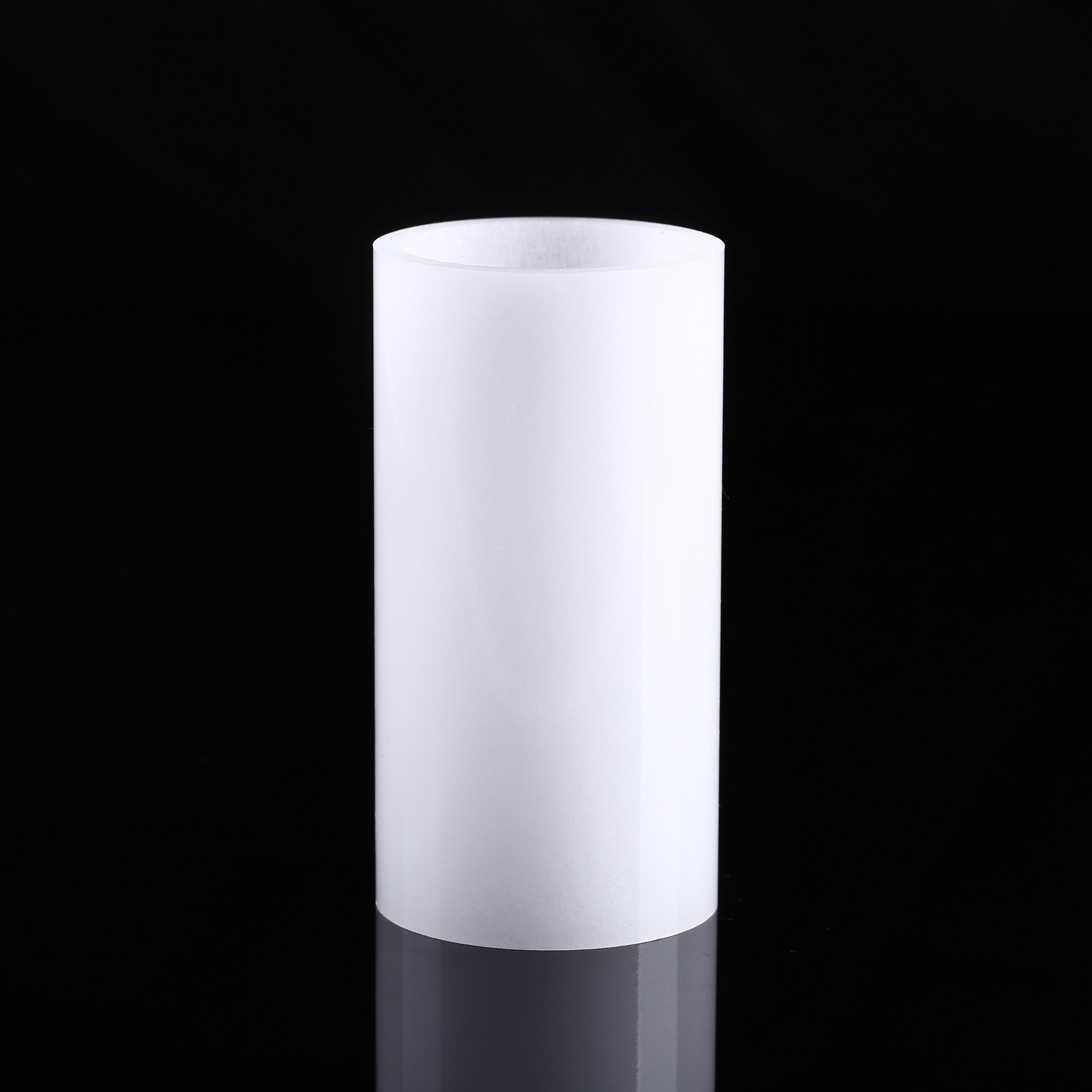
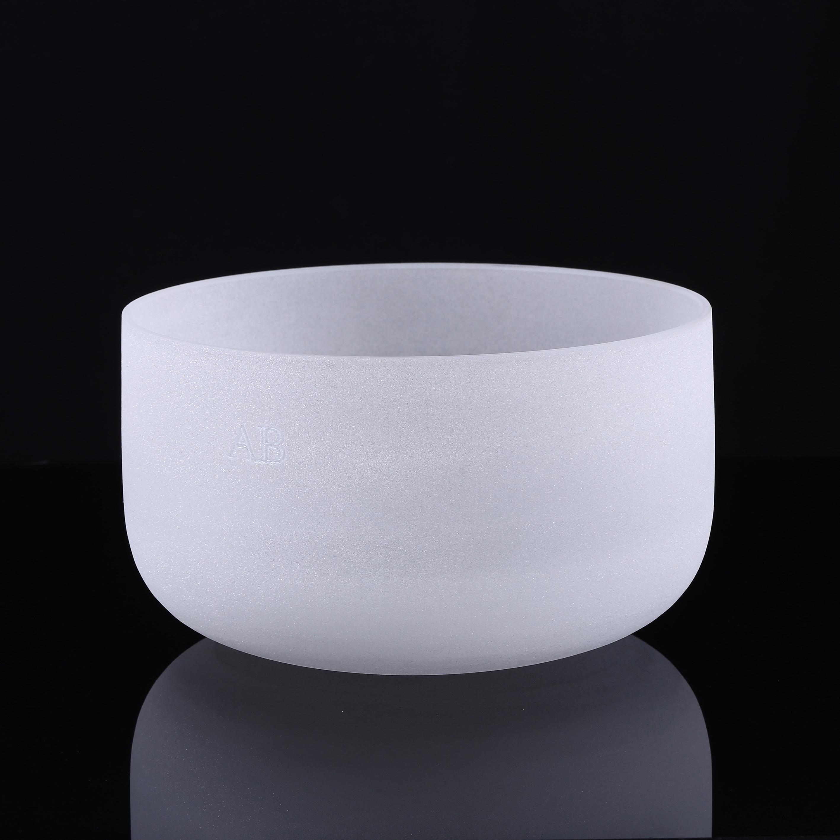
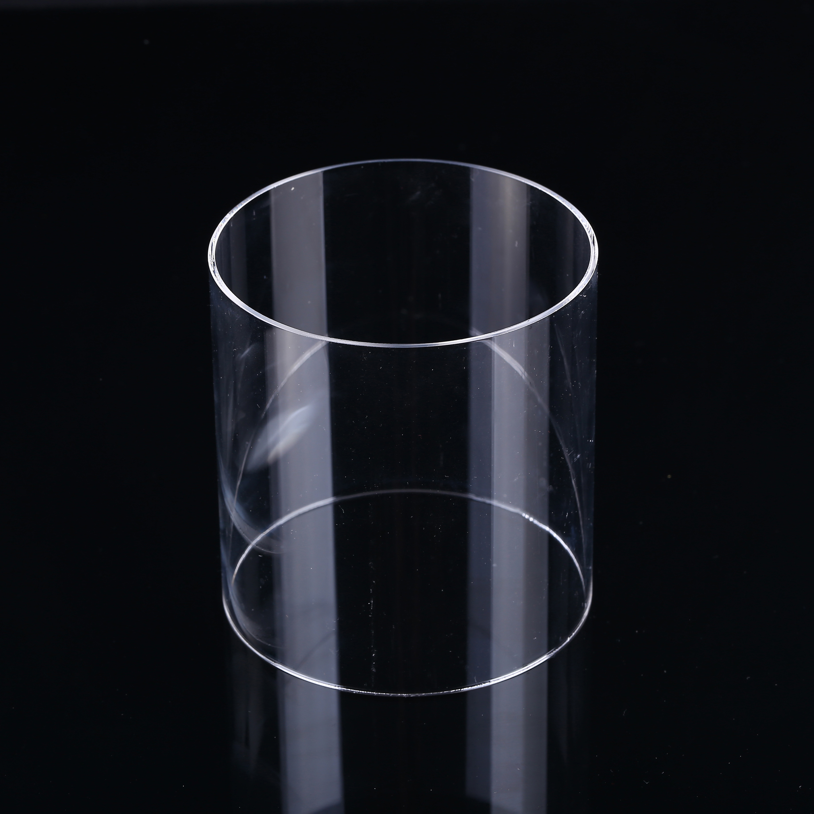
Unlike trading middlemen, Nivra operates full chemical and dimensional inspection loops on site. Utilizing Zygo optical interferometers, laser micrometer gauges, and spectrophotometers spanning 190nm to 3500nm, we verify total thickness variation (TTV < 1µm), surface flatness, bubble-inclusion classes, and chemical purity prior to clearance.
Streamlined Importation into Bangkok & Eastern Seaboard
Step-by-step roadmap for clearing customs at Bangkok Port (Klong Toey), Laem Chabang, and Suvarnabhumi Airport Cargo.
Design & Drawing Review
Share your technical drawings (CAD / DWG / PDF / STEP). Our engineers confirm material grade (JGS1/2/3), dimensional tolerances, surface finish, bevel geometry, and quantity within 5 hours.
Custom Prototype Sign-off
For precision quartz substrates and custom wafer boats, low-volume prototypes (MOQ 1–10 pcs) are machined, measured, and air-couriered to your facility for pilot qualification.
Production & Cleanroom QC
Production takes place under strict in-process tolerance controls. Every component undergoes ultrasonic cleaning, optical laser surface inspection, and serialized batch inspection reporting.
Anti-Moisture Export Packing
Protected by specialized anti-static cleanroom PE bags, micro-cell EPE foam nests, desiccant packs, and heavy-duty fumigation-free wooden crates designed to absorb shock during marine or air transit.
Form E & Fast Clearance
We issue Certificate of Origin Form E (China-ASEAN FTA), allowing Thai customs to apply 0% import duty on HS 7002.31 / 7002.32 / 7020.00 items, facilitating rapid release via Klong Toey or Laem Chabang.
Frequently Asked Questions by Bangkok Industrial Buyers
Direct technical and commercial answers addressing tariffs, tolerances, lead times, and application engineering.
What are the customs duties and tariff codes for importing quartz glass into Thailand from China?
- 7002.31.00: Tubes of fused quartz or other fused silica (0% under Form E).
- 7002.32.00: Tubes of other glass having a linear coefficient of expansion not exceeding 5×10⁻⁶ per Kelvin.
- 7006.00.00: Glass plates, sheets, discs, whether or not worked, edge-ground, polished.
- 7017.10.00: Laboratory, hygienic or pharmaceutical glassware of fused quartz or fused silica.
- 7020.00.00: Other articles of glass (industrial quartz vessels, custom tanks, flanges, crucibles).
How does Nivra Quartz prevent fragile glass breakage during maritime and air transport to Bangkok?
What is the typical shipping lead time from your factory in Donghai to facilities in Greater Bangkok?
How does tropical humidity and high ambient temperature in Thailand affect fused quartz substrates?
Can you produce custom quartz glass substrates and wafer carriers according to CAD drawings?
- High-speed CNC ultrasonic contour milling, internal cavity pocketing, and step profiling.
- Micro-hole laser drilling down to Ø 0.2mm with zero edge chipping.
- Double-sided mechanical lapping and chemical mechanical polishing (CMP) for wafers up to 300mm (12 inches) with Total Thickness Variation (TTV) < 1µm.
- Complex glassblowing, lathe fusing, and welding of flanges, spiraled cooling jackets, and gas distribution manifolds.
What are the continuous and peak thermal thresholds for your quartzware before devitrification occurs?
What is your Minimum Order Quantity (MOQ) for Thai purchasers?
How does Nivra ensure trace metal purity for semiconductor cleanroom operations?
Connect Directly with Nivra's Quartz Engineering Team
Accelerate your procurement pipeline in Thailand. Submit your technical drawings, dimensional tolerances, and material grade specifications. Receive engineering feasibility feedback, price calculations, and logistics planning within 5 hours.