High-Purity Quartz & Fused Silica Substrates for Puebla Industries
Explore factory-calibrated quartz products engineered for semiconductor processing, automotive sensor optics, laser welding shields, and laboratory synthesis.
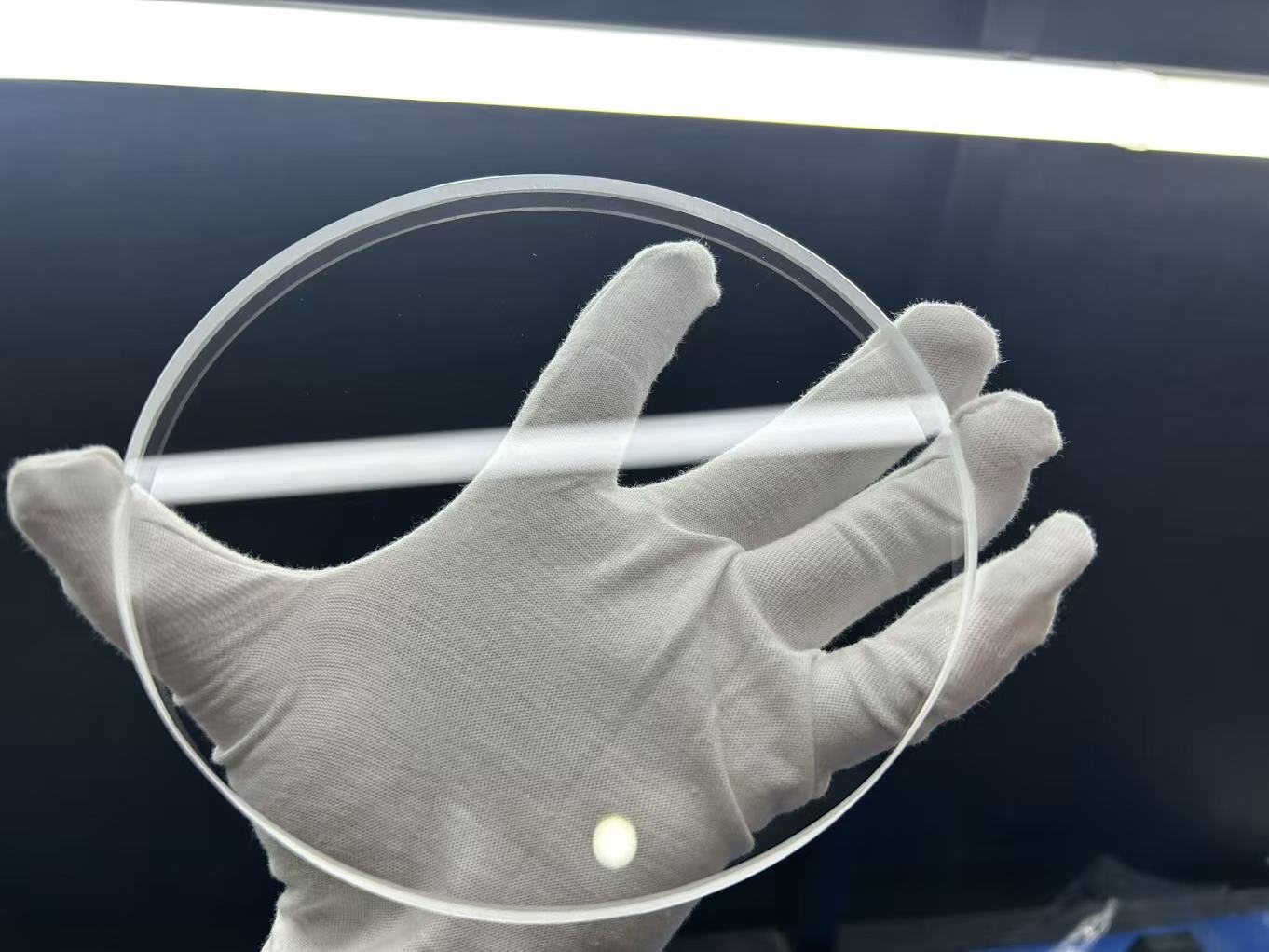
Wholesaler Customized High Quality Clear Fused Quartz Glass Sheet Custom Used in Optics and Photovoltaics
Optical-grade synthetic silica offering >92% transmission across DUV-NIR wavelengths, minimal bubble class, and superior mechanical flatness.
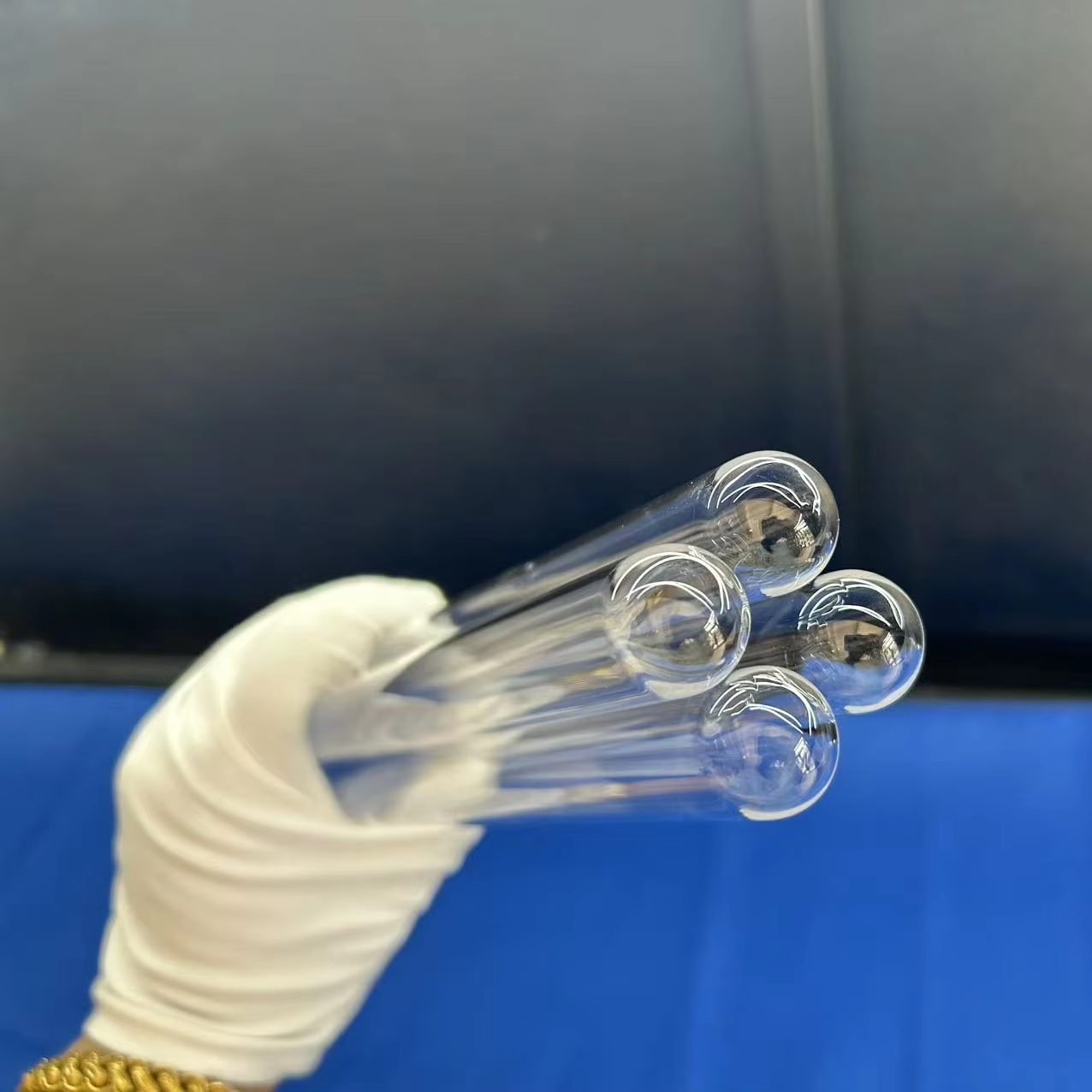
The Factory Produces High-purity Fused Silica Bottom Sealing Tubes with an Diameter of 20-25mm Cutting and Welding Services
Precision sealed bottom tubes designed for chemical deposition, thermal annealing furnaces, and high-vacuum automotive component degassing.
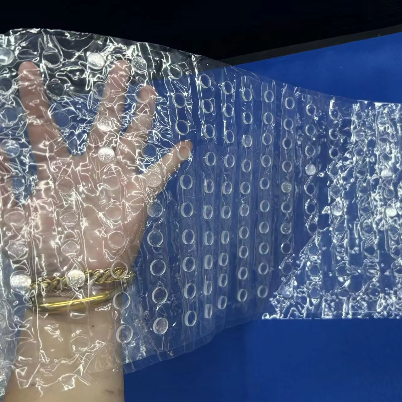
Factory-Made High-purity Small Size Quartz Wafer, Provide Cutting and Polishing Services
Double-side CMP polished fused silica wafers with Ra < 0.5 nm surface roughness, tailored for MEMS, optical sensor lithography, and microfluidics.
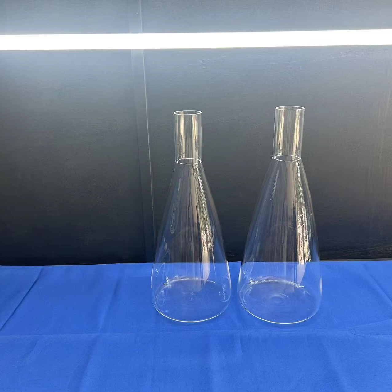
Laboratory Fused Silica Quartz Glass Flask
Continuous 1100°C thermal stability glassware with inert corrosion resistance to aggressive acids, ideal for Puebla university and QA analytical labs.
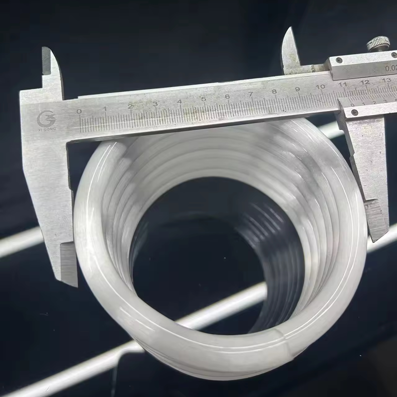
Helical Clear Quartz Glass Coil t Tube
Precision flamed spiral condenser coils providing ultra-efficient thermal exchange and photochemical flow-through in harsh chemical environments.
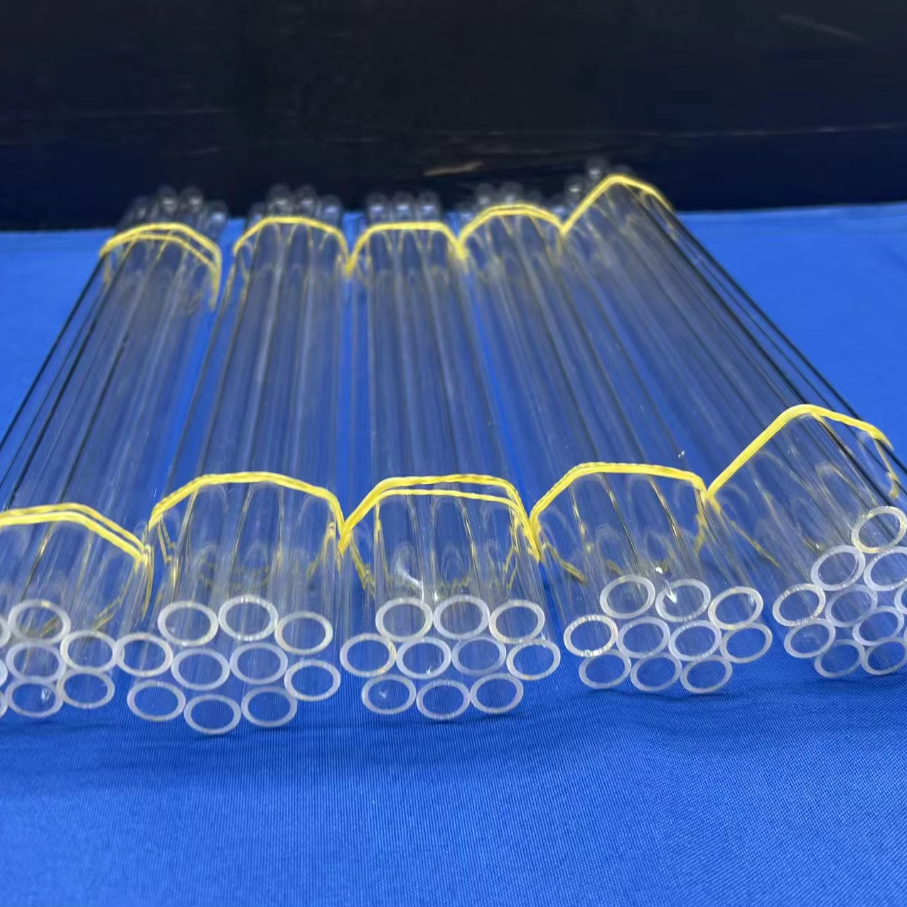
Quartz test Tube
Standard and custom-dimension high-purity test tubes designed to withstand sudden thermal quenching from 1100°C to cold water without fracturing.
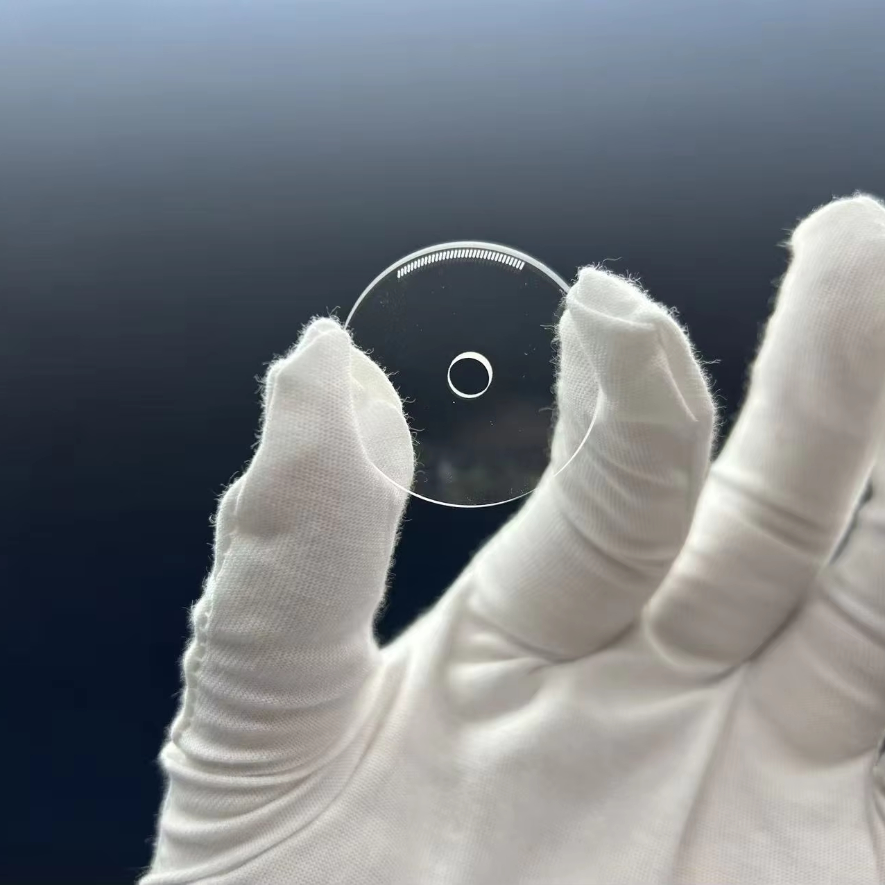
Frosted Quartz Sheet
Uniformly sandblasted or chemical-frosted quartz plates for light diffusion in UV curing systems, automotive illumination testing, and furnace baffles.
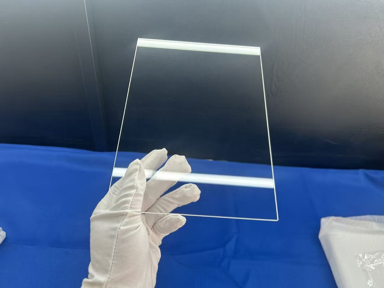
Custom Polished Purity Transparent Square Quartz Glass Plate 3mm Thick Clear Optical Instruments for Welding Cutting
High laser-damage-threshold (LDT) protective inspection windows engineered specifically for fiber laser cutting and automotive welding robotics.
Engineering Superiority: Fused Silica vs. Natural Fused Quartz
A comprehensive engineering guide for materials scientists and procurement teams across Puebla seeking exact optical, thermal, and mechanical material matching.
Synthetic Fused Silica (JGS1 Grade)
Fabricated via the chemical vapor deposition (CVD) or flame hydrolysis of high-purity silicon tetrachloride (SiCl₄), our JGS1 synthetic fused silica achieves total impurity levels under 1 ppm. It guarantees outstanding deep ultraviolet (DUV) spectral transmission down to 185 nm, rendering it virtually bubble-free and free of metallic inclusions for laser optoelectronics and microlithography.
Optical Fused Quartz (JGS2 Grade)
Manufactured by high-temperature fusion of select Donghai natural crystalline quartz, JGS2 optical fused quartz bridges physical durability with wide-spectrum optical clarity (220 nm to 2500 nm). Widely specified across Puebla's industrial automation plants as sight glasses, optical flats, and UV curing substrate panels where cost efficiency and thermal resistance are vital.
Infrared Fused Silica (JGS3 Low-OH Grade)
Electrically fused in a high-vacuum chamber, JGS3 infrared fused quartz eliminates hydroxyl ion (OH⁻) absorption peaks, reducing water content to below 5 ppm. This delivers crystal-clear optical transmittance from 260 nm deep into the mid-infrared band up to 3500 nm, vital for thermal imaging windows, pyrometry, and CO₂/solid-state laser beam diagnostics.
Precision Applications Across Puebla’s Advanced Manufacturing Corridors
From Tier-1 automotive robotics in Cuautlancingo to world-class astrophysics in Tonantzintla, our fused silica components power Puebla's high-precision manufacturing.
Automotive Tier-1 Clusters (Cuautlancingo & San José Chiapa)
Puebla stands as Mexico's premier automotive state, home to one of Volkswagen’s largest plants globally and the Audi México smart facility. In these state-of-the-art facilities, automated fiber laser welding, chassis cutting, and robotic adhesive curing systems operate non-stop. Our custom-dimension JGS1 fused silica laser protection windows and pyrometer sight glasses withstand harsh metal spatters and continuous thermal radiation, preventing catastrophic downtime on critical robotic assembly lines.
Next-Gen LiDAR & ADAS Sensor Validation
As Puebla's automotive supply chain transitions aggressively toward electric mobility and Level 2+/3 autonomous driving components, Tier-1 sensor suppliers require high-precision optical substrates. Our chemically polished fused silica wafers offer an exceptionally low coefficient of thermal expansion (5.5 × 10⁻⁷ /°C) and tight wavefront distortion (λ/10). These characteristics guarantee zero optical aberration across ambient operating temperatures from -40°C to +125°C in vehicular LiDAR transmitters and front-facing camera housings.
Astrophysics & Nanophotonics (INAOE & BUAP Research Hubs)
Puebla is a recognized epicenter of academic and scientific excellence, anchored by the Instituto Nacional de Astrofísica, Óptica y Electrónica (INAOE) in Tonantzintla and the Benemérita Universidad Autónoma de Puebla (BUAP). Our precision-ground fused quartz substrates, spectrometer cuvettes, and vacuum chamber viewports serve advanced laser spectroscopy, nanophotonic waveguides, and quantum optics laboratories requiring verifiable certification, ultra-low fluorescence, and high optical homogeneity.
Photovoltaic & Green Energy Cleanroom Processing
Across Central Mexico's expanding clean-energy initiatives, solar cell producers and battery material developers rely on high-purity thermal tooling. Our bottom-sealing quartz diffusion tubes, quartz boats, and frosted quartz covers withstand sustained operating temperatures up to 1100°C without crystal phase devitrification, completely preventing heavy-metal contamination during high-purity silicon wafer doping and thin-film solar annealing cycles.
Fused Silica Technical Specifications & Optical Grade Matrix
Direct material performance metrics to assist engineering design reviews, tolerances, and international equivalency evaluations.
| Physical / Chemical Property | JGS1 (Synthetic Fused Silica) | JGS2 (Optical Fused Quartz) | JGS3 (Low-OH Infrared Fused Quartz) |
|---|---|---|---|
| Primary Spectral Range | 185 nm – 2500 nm (Deep UV to Vis) | 220 nm – 2500 nm (Standard Optical) | 260 nm – 3500 nm (Near to Mid IR) |
| SiO₂ Purity | ≥ 99.999% | ≥ 99.99% | ≥ 99.99% |
| Hydroxyl Content (OH⁻) | ~ 1200 ppm (Hydrated form) | 150 – 200 ppm | < 5 ppm (Vacuum melted) |
| Density (at 20°C) | 2.20 g/cm³ | 2.20 g/cm³ | 2.20 g/cm³ |
| Thermal Expansion Coeff. (20–300°C) | 5.5 × 10⁻⁷ / K | 5.5 × 10⁻⁷ / K | 5.5 × 10⁻⁷ / K |
| Continuous Max Operating Temp | 1100 °C | 1100 °C | 1150 °C |
| Softening Point | 1730 °C | 1683 °C | 1685 °C |
| Surface Polish Quality (Available) | 20/10 Scratch-Dig, Ra < 0.5 nm | 40/20 Scratch-Dig, Ra < 1.0 nm | 40/20 Scratch-Dig, Ra < 1.0 nm |
| Surface Flatness / Wavefront | λ/10 to λ/4 @ 632.8 nm | λ/4 to 1λ @ 632.8 nm | λ/4 to 1λ @ 632.8 nm |
Nearshoring Dynamics & Optical Sourcing Evolution in Puebla
Analyzing macroeconomic shifts, USMCA supply chain requirements, and direct factory procurement advantages for Central Mexican manufacturers.
Mitigating North American Reseller Markups
Traditionally, manufacturing plants in Puebla's Parque Industrial FINSA, Parque Industrial Puebla 2000, and Ciudad Modelo procured quartz substrates through US or European intermediaries. This created 300% to 500% price inflations and 12-week distribution delays. By partnering directly with our primary processing plant in Donghai, Jiangsu, procurement teams bypass middle-tier distributor markups while securing custom dimensions built to strict OEM drawing tolerances.
Automotive Electrification & Vision Systems
With Puebla accelerating its investments in electric vehicle (EV) platforms and autonomous safety modules, optical component requirements have expanded beyond basic lighting. Today's manufacturing requires thermally resilient optical filter substrates, LiDAR protective sight glasses, and battery welding pyrometer viewports capable of continuous 24/7 robotic operation without optical degradation or clouding under heat stress.
Streamlined Logistics via Veracruz & AICM
Puebla’s strategic geographical location between the Port of Veracruz (280 km east via highway 150D) and Mexico City's cargo airports (AICM/AIFA) allows seamless international transit. Bulk quartz orders clear customs rapidly through Veracruz ocean terminals, while emergency prototype shipments arrive via express airfreight directly to Puebla’s industrial corridor in under 6 business days with complete breakage guarantees.
Why Global & Puebla Buyers Choose Nivra Quartz
Operating from Donghai County, China's world-renowned quartz epicenter, we combine raw crystal synthesis with advanced optical fabrication.
101–200 Skilled Specialists
Founded in 2019, our workforce combines master glassblowers with CNC optical polishing engineers, ensuring that intricate quartz modifications comply strictly with customer drawings.
Rapid 5-Hour Response
With an audited 88.89% immediate inquiry rate, our technical sales engineers review CAD drawings (STEP, DWG, DXF, PDF) and confirm manufacturability within 5 hours.
Zero-Breakage Packaging
Every substrate is individually sealed, bathed in custom shock-absorbing closed-cell EPE foam, and encased within heavy-gauge, fumigation-free wooden export crates.
Complete Traceability
Each delivery includes batch certificates of analysis (COA), spectrophotometer transmission curves, and interferometric wavefront inspection reports upon request.
Frequently Asked Questions: Sourcing Fused Silica Substrates for Puebla
Addressing international trade, customs handling, quality inspection, and technical grade selection for Mexican buyers.
How do you handle shipping, customs clearance, and Incoterms (CIF, DAP, DDP) to Puebla, Mexico?
We routinely supply engineering clients throughout Mexico. For seafreight container and LCL consignments, shipments sail directly from Qingdao or Shanghai to the Port of Veracruz (conveniently situated only 280 km from Puebla via federal toll highway 150D) or the Port of Manzanillo for Pacific logistics. Customs clearance can be managed via your local customs broker (Agente Aduanal), or we can coordinate door-to-door delivery under DAP or DDP (Delivered Duty Paid) Incoterms. For urgent prototypes, small batches, or emergency replacement laser windows, we ship via DHL, FedEx, or UPS Priority directly to your facility in Cuautlancingo, San José Chiapa, or Puebla City within 4 to 7 business days, providing complete customs documentation including commercial invoices, packing lists, and Mexican HS code classifications (typically 7002.31 or 7002.39).
What is the difference between JGS1, JGS2, and JGS3, and which should our Puebla engineers select?
Selection depends entirely on your system's operational wavelength and thermal requirements:
• JGS1 (Synthetic Fused Silica): Choose JGS1 for deep ultraviolet applications (185 nm – 2500 nm), high-power industrial excimer or fiber lasers, UV-curing lithography, and medical photonics. It has virtually no bubbles or impurities, zero fluorescence, and maximum laser-induced damage thresholds (LDT).
• JGS2 (Optical Fused Quartz): Standard optical grade (220 nm – 2500 nm) fabricated from refined natural quartz. Perfect for standard automotive sight glasses, furnace inspection ports, and optical instrumentation where high UV transmission below 220 nm is not needed.
• JGS3 (Infrared Grade): Characterized by vacuum-desorbed hydroxyl ions (< 5 ppm OH⁻). If your application involves thermal pyrometry, CO₂ laser processing, or infrared detection from 2000 nm to 3500 nm, JGS3 eliminates the severe absorption dip found in standard silica at 2730 nm.
How does Nivra Quartz guarantee zero breakage during intercontinental transit to Central Mexico?
Exporting high-precision, fragile optical substrates requires proven engineered packaging. Each quartz plate or wafer is washed in ultrasonic deionized baths, wrapped in particulate-free cleanroom tissue, sealed in vacuum-sealed antistatic pouches, and housed in high-density customized EPE (expandable polyethylene) die-cut foam trays. These trays are suspended within rigid, dual-wall fluted corrugated cartons, which are then placed into treated, fumigation-free solid timber export crates with external shock and tilt indicators. In the rare event of transit damage documented upon initial delivery inspection, our immediate replacement policy guarantees remanufacturing and replacement dispatch at zero additional expense to your company.
Can you manufacture non-standard quartz shapes, precision hole-drilling, and beveled edges from CAD drawings?
Yes. Over 65% of our fabrication orders are bespoke OEM fabrications. Our facility operates multi-axis CNC glass machining centers, ultrasonic core drills, double-sided chemical-mechanical polishing (CMP) platforms, and robotic laser cutting equipment. We routinely deliver tight tolerances: dimensional tolerances down to ±0.05 mm, thickness tolerances to ±0.02 mm, mechanical bevels (C-cut or round edges to prevent edge chipping), stepped substrate shoulders, ultrasonic micro-holes from 0.5 mm diameter, and ground or fire-polished finishes according to your CAD drawings (DWG, DXF, STEP, or PDF).
What quality inspection documentation and compliance certificates are included with commercial orders?
Quality consistency is fundamental to automotive and cleanroom qualification. With each production batch, we can furnish:
1. Certificate of Analysis (COA): Confirming 99.99% or 99.999% SiO₂ purity and residual trace metal assays (Fe, Al, Ti, Na, Ca, Cu, K ppm counts).
2. Optical Transmission Spectra: Verified spectrophotometer curves showing spectral transmittance from 190 nm through 3200 nm.
3. Dimensional & Surface Flatness Reports: Non-contact optical metrology measuring surface roughness (Ra), parallelism, and wavefront distortion (λ/4 or λ/10).
4. Environmental Compliance: Full compliance documentation for RoHS, REACH, and non-conflict mineral declarations required for USMCA Tier-1 audits.
What are your Minimum Order Quantities (MOQ) and production lead times for delivery to Puebla?
To support academic research at INAOE/BUAP as well as industrial prototyping for Puebla Tier-1 suppliers, standard substrate MOQs start at just 1 to 10 pieces for standard stock dimensions. Custom CNC-machined wafers and optical discs typically maintain an MOQ of 20 to 50 pieces. Production turnaround for prototypes is normally 7 to 10 working days, while volume production batches (500–5,000 pieces) require 2 to 3 weeks prior to express air or consolidated ocean dispatch.
Accelerate Your Quartz Sourcing in Puebla Today
Send your CAD drawings, dimensional specifications, or required optical grades directly to our engineering desk. Receive verified material recommendations, formal quotations, and manufacturing lead times within 5 business hours.