Verified High-Purity Fused Quartz Components & Crucibles
Manufactured from ultra-pure natural and synthetic silicon dioxide (SiO₂ ≥ 99.99%), rigorously tested for Czochralski (CZ) pulling, photovoltaic ingot synthesis, chemical vapor deposition (CVD), and precision optical processing.
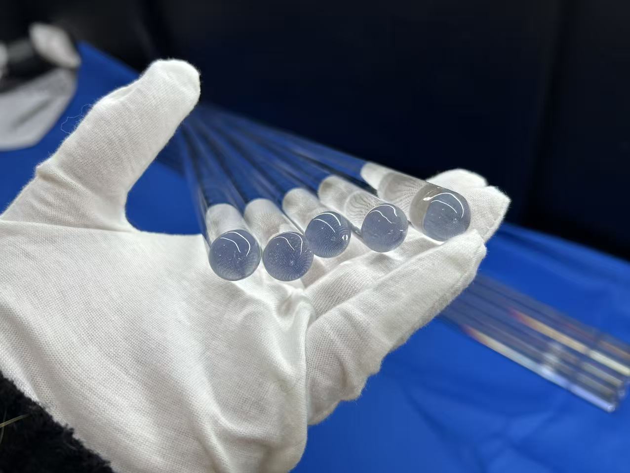
High-Purity Fused Quartz Round Rods (Cutting, Welding & Bending)
Technical Details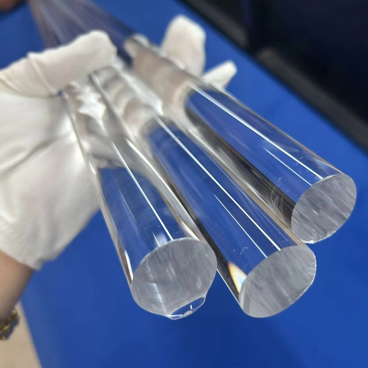
Large Diameter Fused Quartz Round Rods for Custom Machining
Technical Details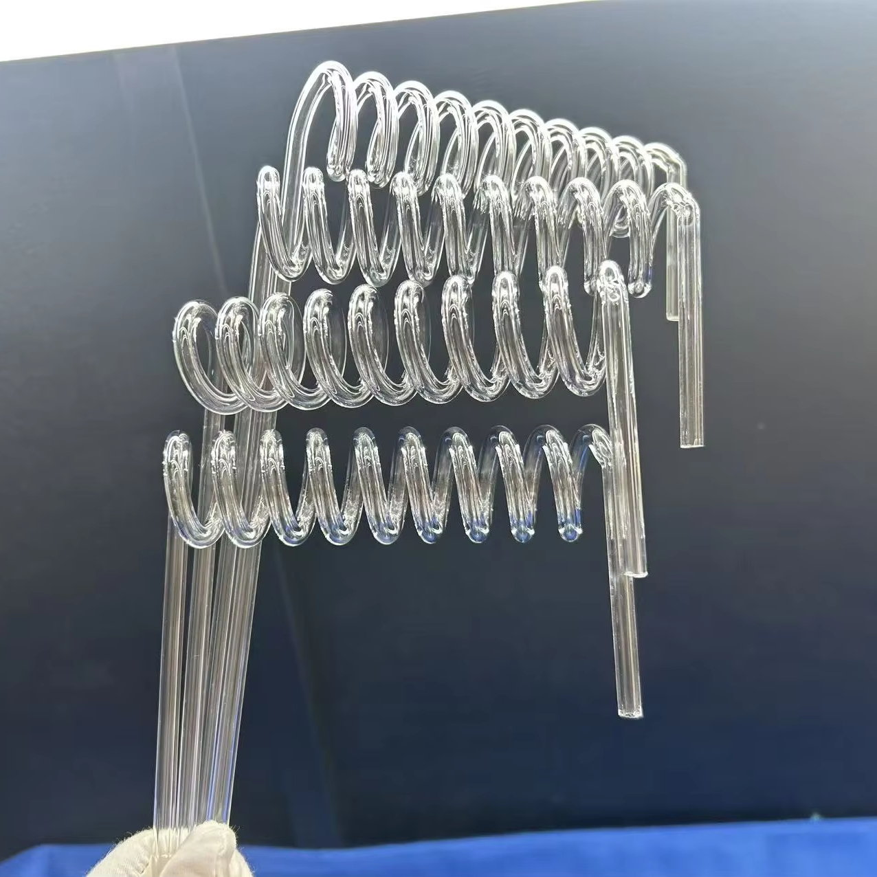
Clear Quartz Spiral Condensation Tube for Advanced Laboratory Use
Technical Details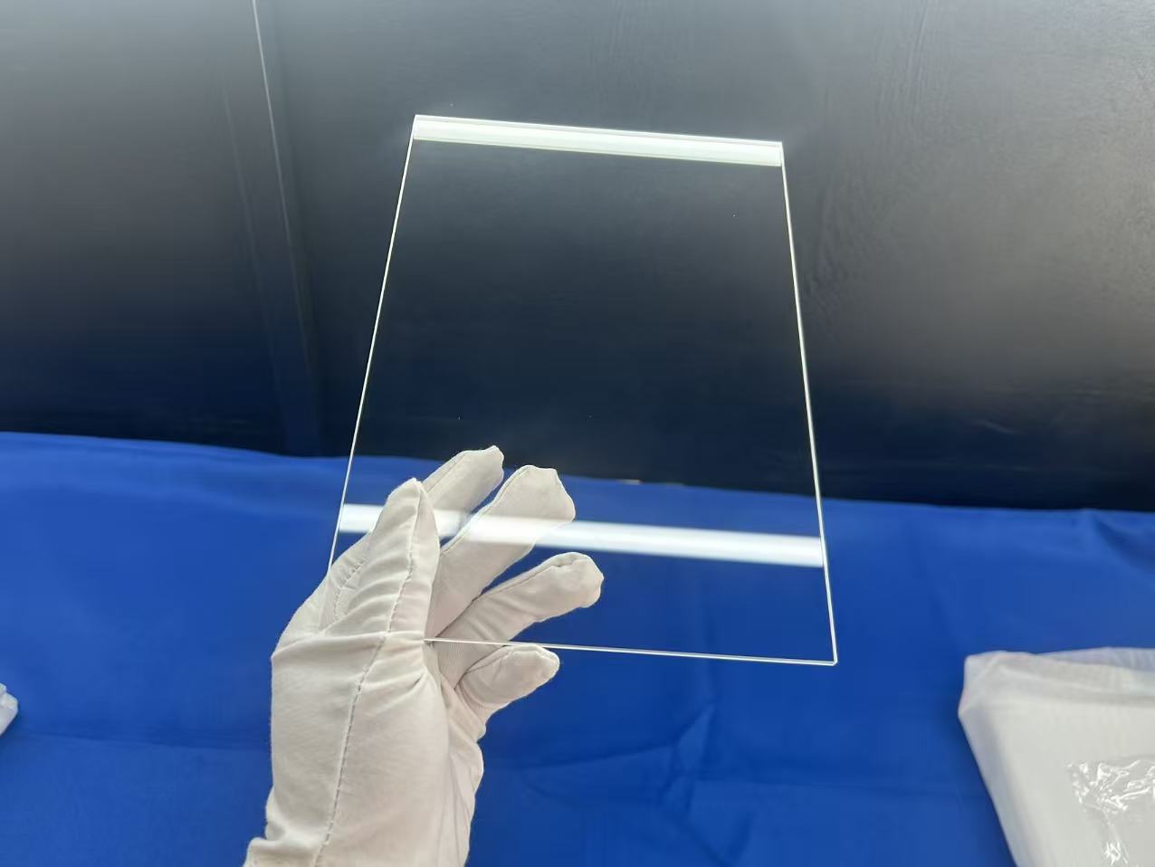
Precision Polished Transparent Square Quartz Plate (3mm Optical Clear)
Technical Details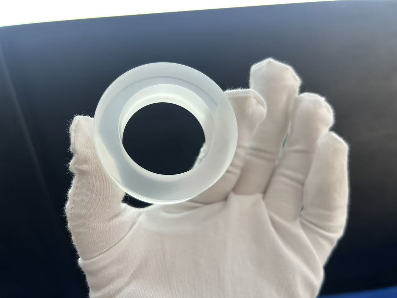
High-Precision CNC Machined Fused Silica Retaining & Sealing Ring
Technical Details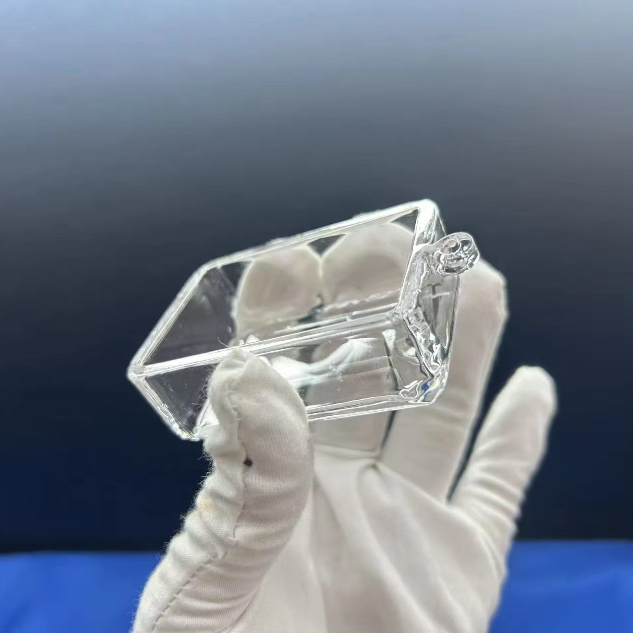
Heavy-Duty Seamless Welded Quartz Tank for Chemical Cleaning
Technical Details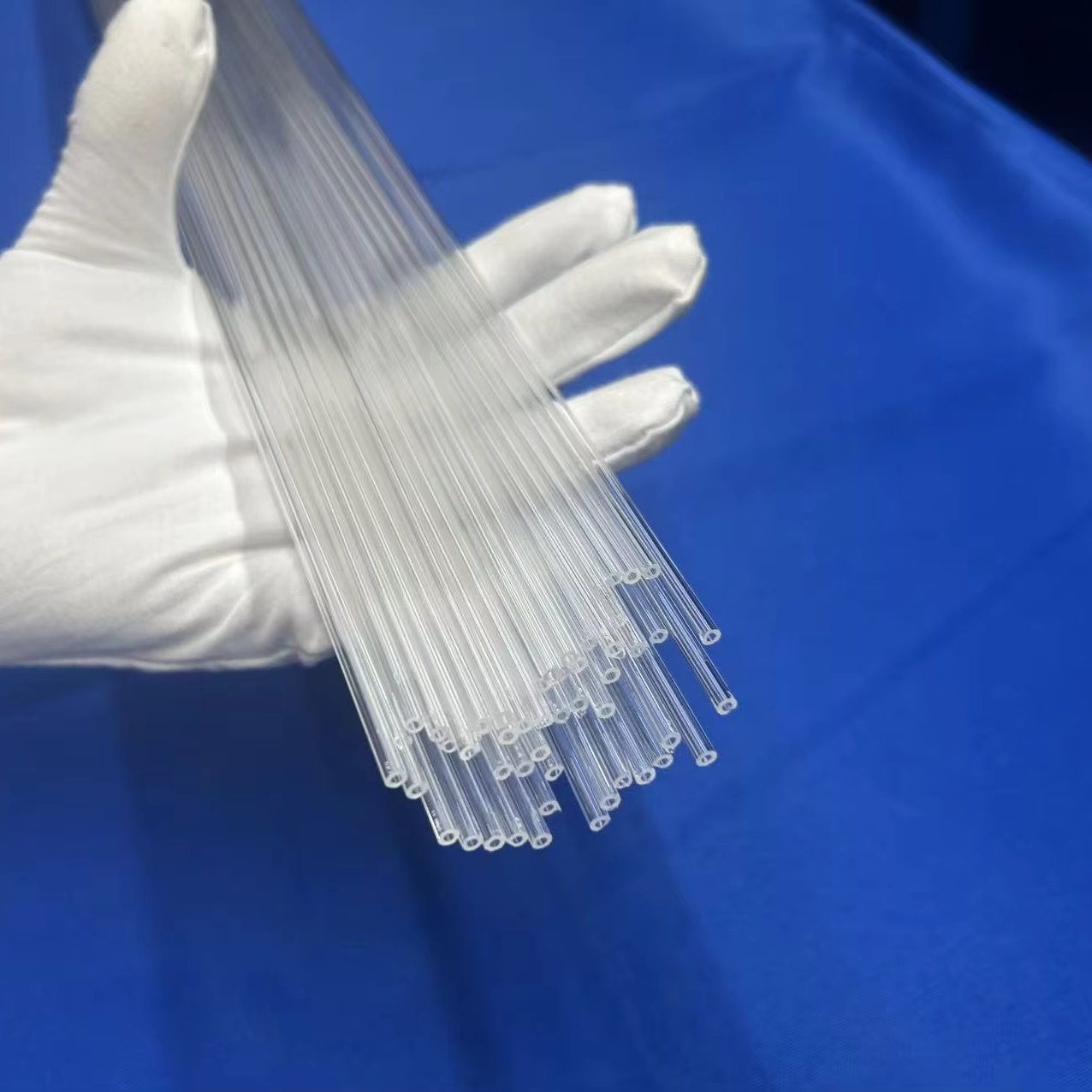
Precision Bore Capillary Quartz Tubing for Fiber Optics & Chromatography
Technical Details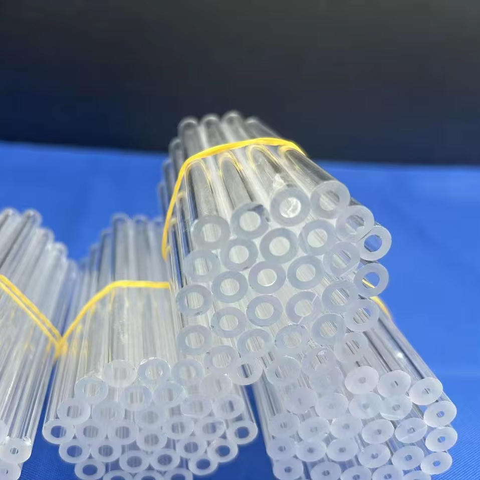
Customized Size High-Temp Clear Quartz Tube for BET Surface Analysis
Technical DetailsDonghai Nivra Quartz Operational Benchmarks
Established in China's quartz heartland, our plant balances high-volume precision hot-end fusing with automated cold machining.
Executive Whitepaper: The Materials Science of Fused Silica Crucibles
In high-temperature metallurgy, semiconductor ingot pulling (Czochralski CZ method), and photovoltaic polysilicon crystal growth, the fused silica crucible represents an indispensable, mission-critical containment vessel. Operating at sustained furnace temperatures exceeding 1420°C to 1550°C in direct contact with molten silicon, the chemical stability, phase transformation kinetics, and impurity profile of the crucible directly determine silicon crystal yield, dislocation density, and minority carrier lifetime.
A trusted fused silica crucible factory must navigate severe physical constraints: molten silicon is highly aggressive, chemically dissolving the inner SiO₂ crucible wall according to the interface reaction: Si (l) + SiO₂ (s) → 2 SiO (g). As silicon monoxide vapor volatilizes, trace impurities embedded within the crucible substrate—such as Aluminum (Al), Iron (Fe), Titanium (Ti), and alkali metals (Lithium, Sodium, Potassium)—leach directly into the melt. In solar cell manufacturing, particularly for TOPCon and Heterojunction (HJT) N-type wafers, excessive alkali contamination catastrophic causes degradation of electrical efficiency. Therefore, understanding raw sand beneficiation, rotary electric-arc fusion, and crystallization dynamics is the hallmark of professional strategic procurement.
Critical Thermodynamic Parameters & Devitrification Dynamics
Clear fused silica (vitreous SiO₂) is thermodynamically unstable below 1710°C; it exists as a meta-stable supercooled liquid. At elevated operational temperatures (>1200°C), fused silica undergoes devitrification, progressively converting into crystalline β-cristobalite. During furnace cooldown, β-cristobalite transitions displacively to α-cristobalite at approximately 220°C to 270°C, accompanied by an instantaneous 3.8% to 5.0% volume contraction that causes structural spalling, micro-fracturing, and catastrophic crucible disintegration.
Premier crucible factories counteract premature devitrification through two distinct thermodynamic strategies:
- Inner Layer Purity Engineering: Utilizing synthetic quartz precursors or ultra-refined natural quartz (total metallic impurities < 8 ppm) on the inner wall to prevent catalytic nucleation points. Alkali metals act as network modifiers that drastically accelerate crystallization; reducing Li, Na, and K to sub-ppm levels ensures a pristine, mirror-like dissolution surface.
- Engineered Micro-Devitrification (Barium Doping): In long-duration solar CZ recharging setups, selected outer or intermediate layers are subtly coated or doped with barium (Ba) compounds. This intentionally induces a uniform, dense, microcrystalline cristobalite barrier layer that prevents deep structural wall softening and deformation under hydro-static silicon pressure.
| Crucible Classification | Manufacturing Process | Impurity Level (Total Metals) | Continuous Temp Limit | Primary Industrial Application |
|---|---|---|---|---|
| Electric Arc-Fused (Natural) | Centrifugal rotation + graphite arc fusion | < 15 – 25 ppm | 1150°C (1450°C short-term) | Standard Photovoltaic Mono-Si Ingot Pulling |
| Synthetic Inner-Layer Arc Fused | Dual-layer arc casting (synthetic SiO₂ liner) | < 5 – 8 ppm (Inner < 0.5 ppm) | 1200°C (1500°C short-term) | N-Type TOPCon / HJT Solar & Semiconductor IC |
| Slip-Cast Sintered Fused Silica | Aqueous slip casting + high-temp ceramic firing | < 50 – 100 ppm | 1100°C (1350°C short-term) | Polysilicon Ingot Casting, Metal Melting, Glass |
| High-Purity Optical Synthetic | Direct chemical vapor deposition (SiCl₄ oxidation) | < 0.1 – 1.0 ppm (Metal Free) | 1250°C (1550°C short-term) | Compound Semi (GaAs, InP), High-Energy Optics |
Comprehensive Comparison: Trace Chemical Impurities & Thresholds
The table below provides maximum tolerable contamination thresholds commonly specified by global procurement departments for Tier-1 semiconductor and photovoltaic crucible sourcing. Values are quantified via Inductively Coupled Plasma Mass Spectrometry (ICP-MS).
| Element Symbol | Impurity Name | Standard PV Grade (ppm) | Semiconductor 28nm–7nm Grade (ppb) | Physical Impact on Melt & Silicon Ingot |
|---|---|---|---|---|
| Al | Aluminum | 6.0 – 12.0 | ≤ 100 | Modifies quartz viscosity; causes P-type counter-doping. |
| Fe | Iron | 0.1 – 0.5 | ≤ 10 | Severe carrier lifetime degradation; defect nucleation. |
| Ti | Titanium | 1.0 – 3.0 | ≤ 15 | Creates deep recombination centers in silicon lattice. |
| Na / K / Li | Alkali Metals | < 0.5 cumulative | ≤ 5 each | Triggers uncontrolled cristobalite devitrification & bubble swelling. |
| Cu / Ni / Cr | Transition Metals | < 0.05 cumulative | ≤ 1 cumulative | Rapid diffusion into gate oxides; causes dielectric breakdown. |
| OH⁻ | Hydroxyl Content | < 30 ppm | < 5 – 10 ppm | Directly lowers glass strain/annealing points, inducing wall sag. |
Donghai County Nivra Quartz Industrial Advantages
Situated in Donghai County, China's world-recognized silicon and quartz industrial cluster, our manufacturing base integrates raw raw sand beneficiation, vacuum sintering, flame processing, precision machining, and cleanroom packaging.
Donghai Direct Supply
Direct proximity to major mineral refining plants reduces domestic freight latency, guarantees rapid sand replenishment, and delivers substantial cost savings on volume purchases.
Full In-House Cold & Hot Processing
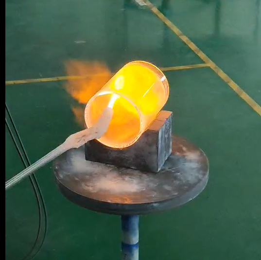
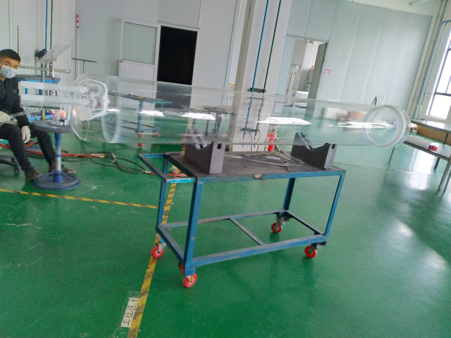
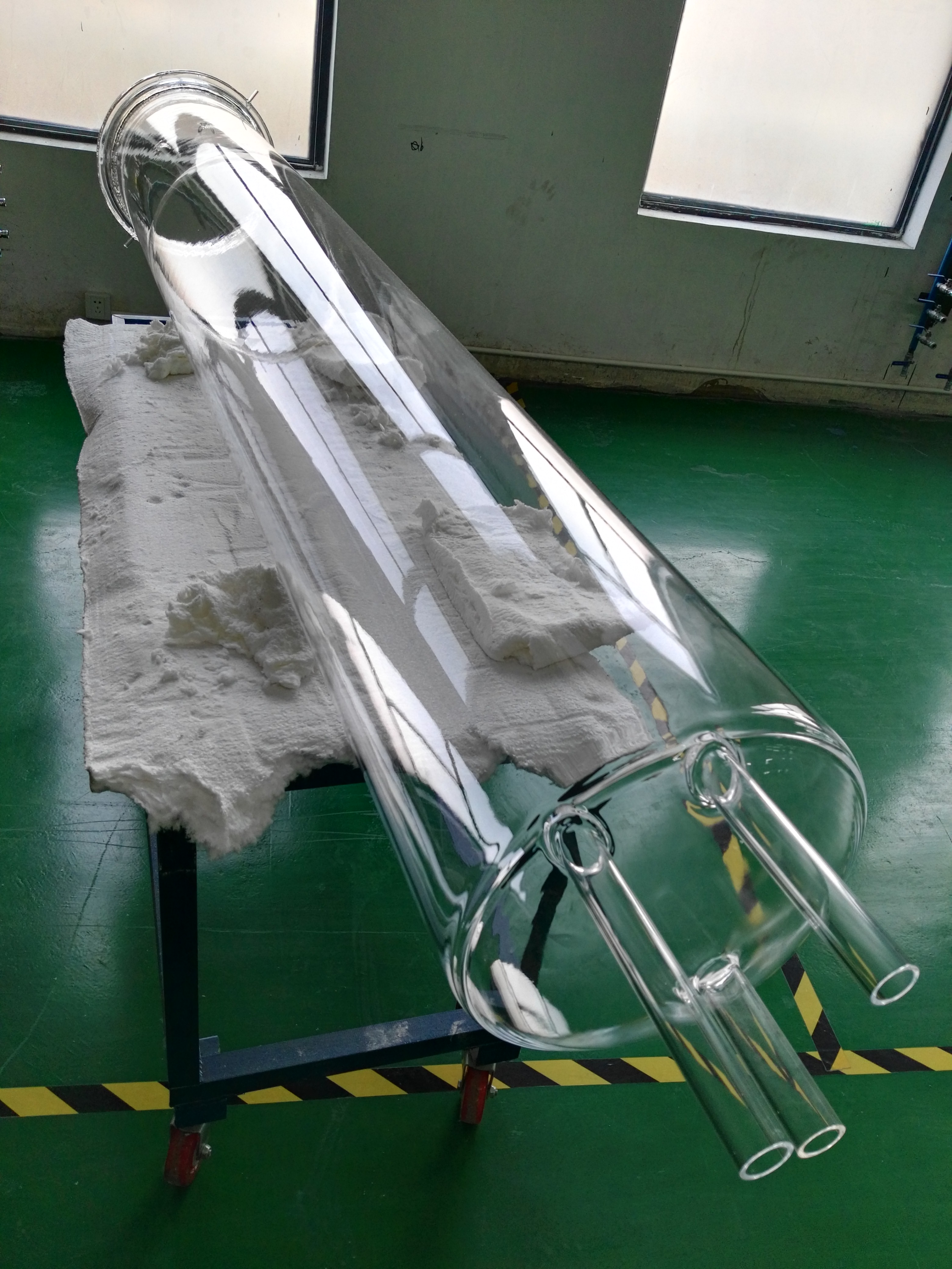
From electric arc rotary melting to 5-axis CNC diamond grinding, flame-polishing, annealing, and ultrasonic acid washing, all production stages remain strictly within company boundaries.
Third-Party On-Site Audit
Premises at 285 Heping East Road have passed comprehensive verification by international inspection agencies. Legal licensing, export documentation, and QA regimes are pre-vetted.
Export Shockproof Packaging
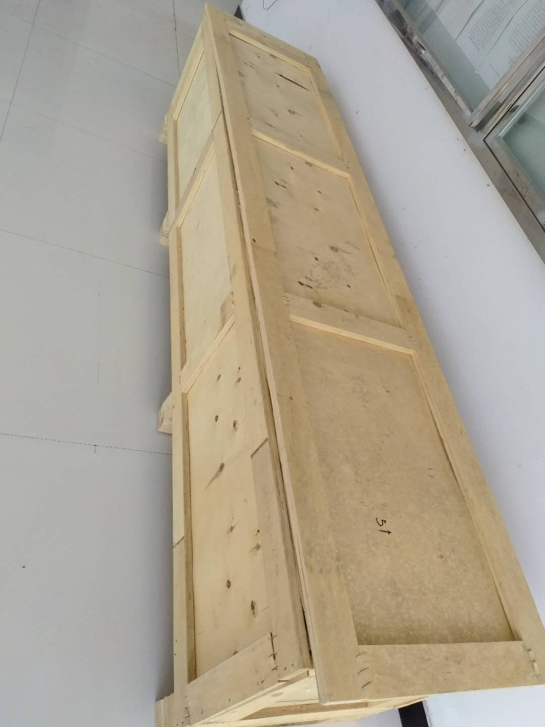
Every component is packed in customized PE cleanroom bags, immobilized by tailored high-density EPE foam cradles, and crated in compliant, fumigation-free reinforced plywood boxes.
International Auditing & Certification Archive
Future Sourcing & Technology Trends in Fused Silica Crucibles
Key evolutions driving wafer economics, furnace longevity, and crucible material selection over the 2025–2030 timeframe.
Transition to 36-Inch to 44-Inch Large Crucibles
Driven by the transition toward G12 (210mm) monocrystalline wafers and long multi-pull recharging systems (Continuous Czochralski, CCZ), standard 28" and 32" crucibles are being displaced. Factories require specialized, massive high-power centrifugal electric-arc equipment capable of maintaining wall uniformity ±1.0 mm across giant 40-inch profiles.
Synthetic Inner-Layer Co-Deposition
As N-type TOPCon, HJT, and interdigitated back contact (IBC) cells push solar conversion efficiencies beyond 25.5%, zero-bubble synthetic SiO₂ inner linings (0.5 mm – 1.8 mm thick) have evolved from an exotic semiconductor option into an absolute requirement to arrest crystal dislocation.
Extended Multi-Recharging Crucible Lifespans
Furnace operational cycles now regularly reach 300 to 450 hours per crucible, with 5 to 10 sequential polysilicon re-chargings. Sourcing managers now prioritize crucible "inner wall corrosion rate per hour" over simple unit purchase price, calculating Total Cost of Ownership (TCO) per kilogram of silicon pulled.
Consult Our Technical Engineering Team for Custom Crucible Design
Send your dimensional drawings (PDF, STEP, or DWG) along with process parameters (furnace temperature profile, vacuum level, melt duration). We provide comprehensive DFM feedback and full material certification within 5 hours.
Crucible Failure Mode Analysis & In-Process Inspection
How tier-1 quartz fabricators prevent thermal cracking, bubble delamination, and melt contamination during demanding manufacturing runs.
Inner-Wall Bubble Expansion & Peeling
Sub-surface micro-bubbles expand exponentially under high vacuum (< 10 mbar) and 1450°C heat. If bubbles burst, quartz debris falls directly into the melt, immediately causing mono-crystal ingot loss. Nivra utilizes high-vacuum arc melting to produce an inner bubble-free zone (BFZ) exceeding 1.5mm thickness.
Premature Wall Sagging & Deformation
Excessive hydroxyl (OH⁻) content acts as a lattice terminating agent, reducing the softening point below 1600°C. Our thermal de-hydroxylation vacuum baking protocols depress OH⁻ levels below 20 ppm, ensuring the crucible retains structural verticality under 400+ kg of silicon mass.
Black Spot Defect Inclusions
Micro-particulate tungsten, iron, or carbon contamination from arc electrodes can form embedded conductive black inclusions. Every crucible manufactured at our facility undergoes high-intensity laser transillumination scanning to eliminate inclusion risks.
Fused Silica Crucible Procurement FAQs
Authoritative answers to the most common technical questions posed by procurement engineers and factory directors.
What is the functional difference between natural fused quartz and synthetic fused silica crucibles?
How do you manage thermal shock resistance in fused silica crucibles?
Can Nivra Quartz produce custom crucibles and labware directly from our CAD drawings?
What are the Minimum Order Quantities (MOQ) and sample lead times?
What testing documentation is delivered with each production lot?
How do you ensure fragile quartz products do not shatter during sea or air transit?
What causes fused quartz crucibles to soften or sag in furnace environments?
What is your measured response rate and communication speed for technical RFQs?
Initiate Your Custom Fused Silica Crucible Project
Partner directly with a certified Donghai manufacturing powerhouse. From single prototyping runs to sustained containerload shipments, we deliver precision dimensional tolerances, industry-low impurity levels, and reliable export logistics.