Featured Semiconductor Quartz Products & Carriers
Manufactured directly at our Donghai facility using synthetic and high-purity natural silica (SiO₂ ≥ 99.99%). Every component delivers exceptional dimensional stability, sub-micron slot pitch tolerances, and thermal shock resistance up to 1,450°C.
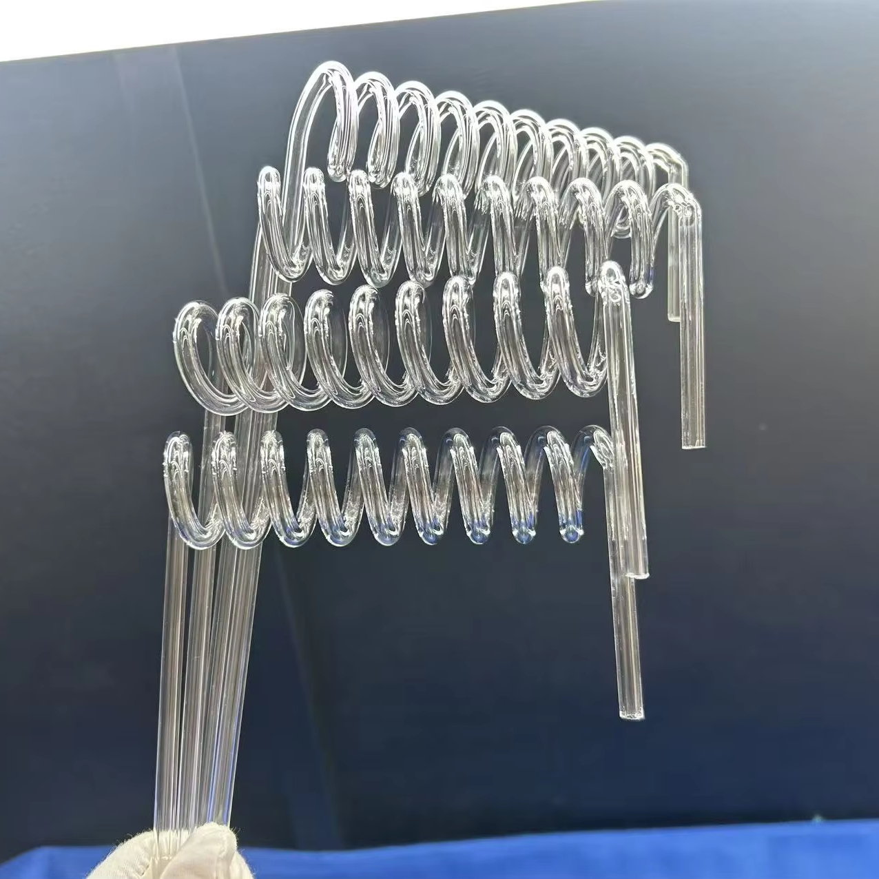
Clear Quartz Spiral Tube for Optics Laboratory Use with Moulding and Bending Services
Custom helical fused silica coils engineered for specialized condenser coils, plasma spectrometers, and high-temperature optical excitation setups. High thermal shock threshold with continuous 1,100°C resistance.
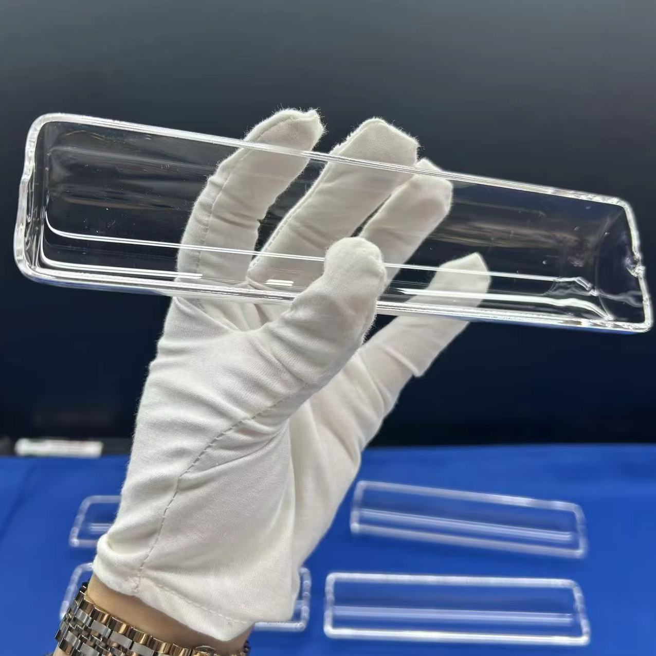
Customized Clear Fused Silica Quartz Boat Polished Clear Quartz Wafer Carrier
SEMI-compliant horizontal and vertical wafer carriers designed for LPCVD, oxidation, and diffusion furnaces. Features CNC-milled tooth profiles with Ra < 0.2 μm fire polishing to eliminate wafer edge chipping.
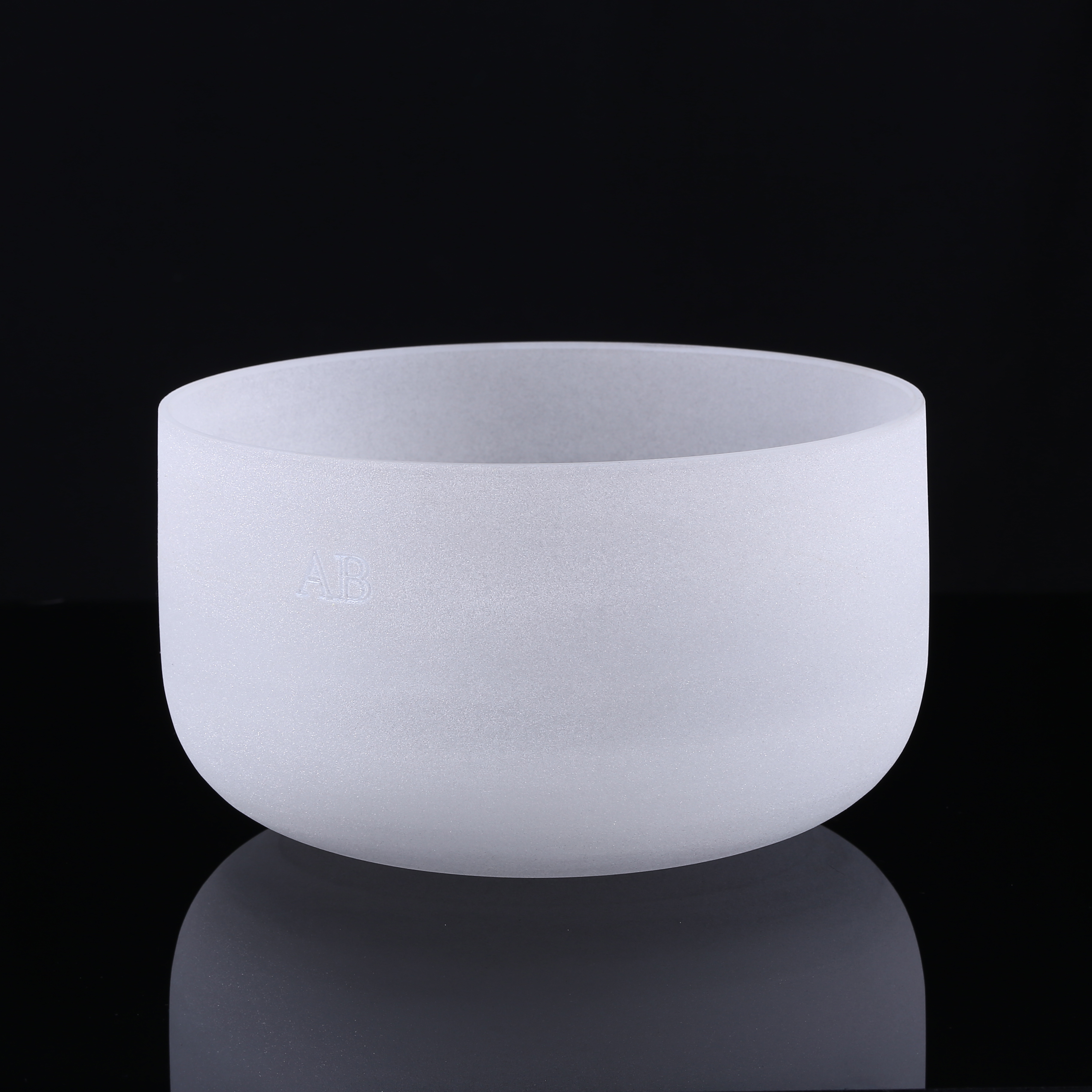
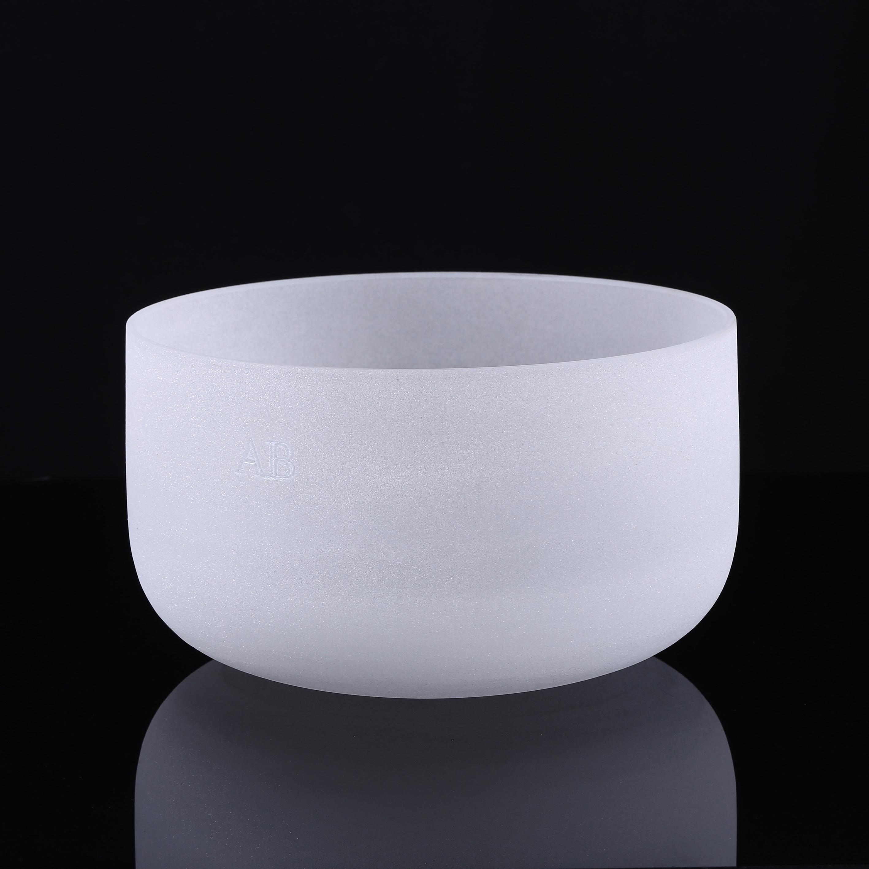
High Temperature Fused Silica Quartz Crucible
High-vacuum electric arc melted fused silica crucibles engineered for semiconductor silicon pulling, PV crystal growth, and metallurgical ashing. Low thermal expansion minimizes thermal runaway risks.
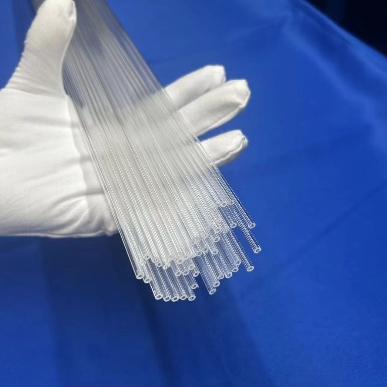
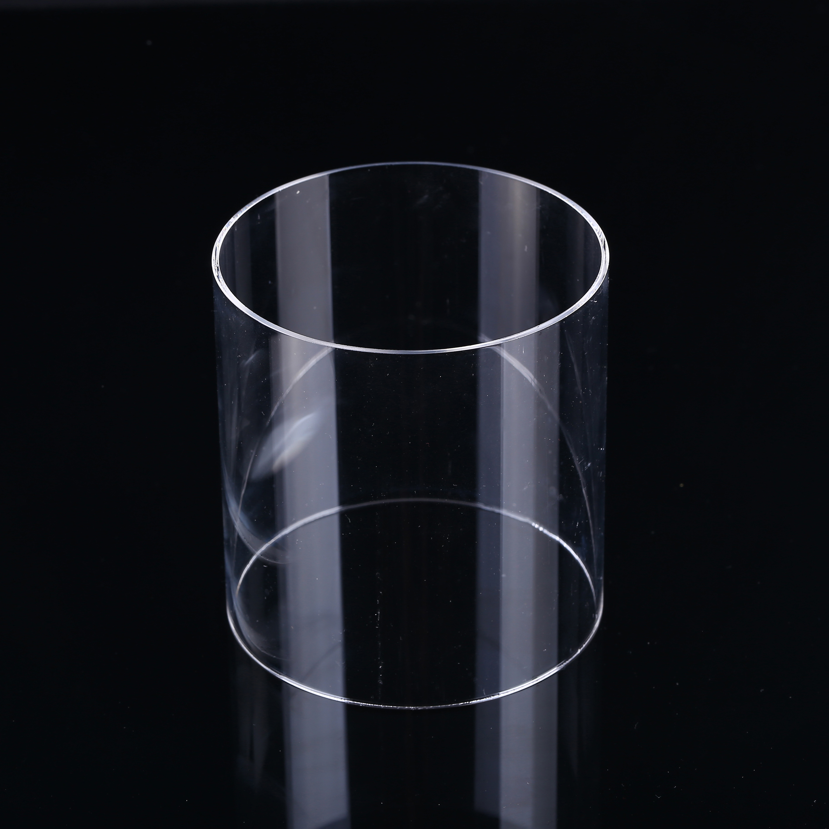
Capillary Quartz Tube
Ultra-narrow bore fused quartz capillary tubes featuring high wall uniformity and tight ID/OD tolerances (±0.01 mm). Suited for gas injection nozzles, chromatography columns, and semiconductor sensor sleeves.
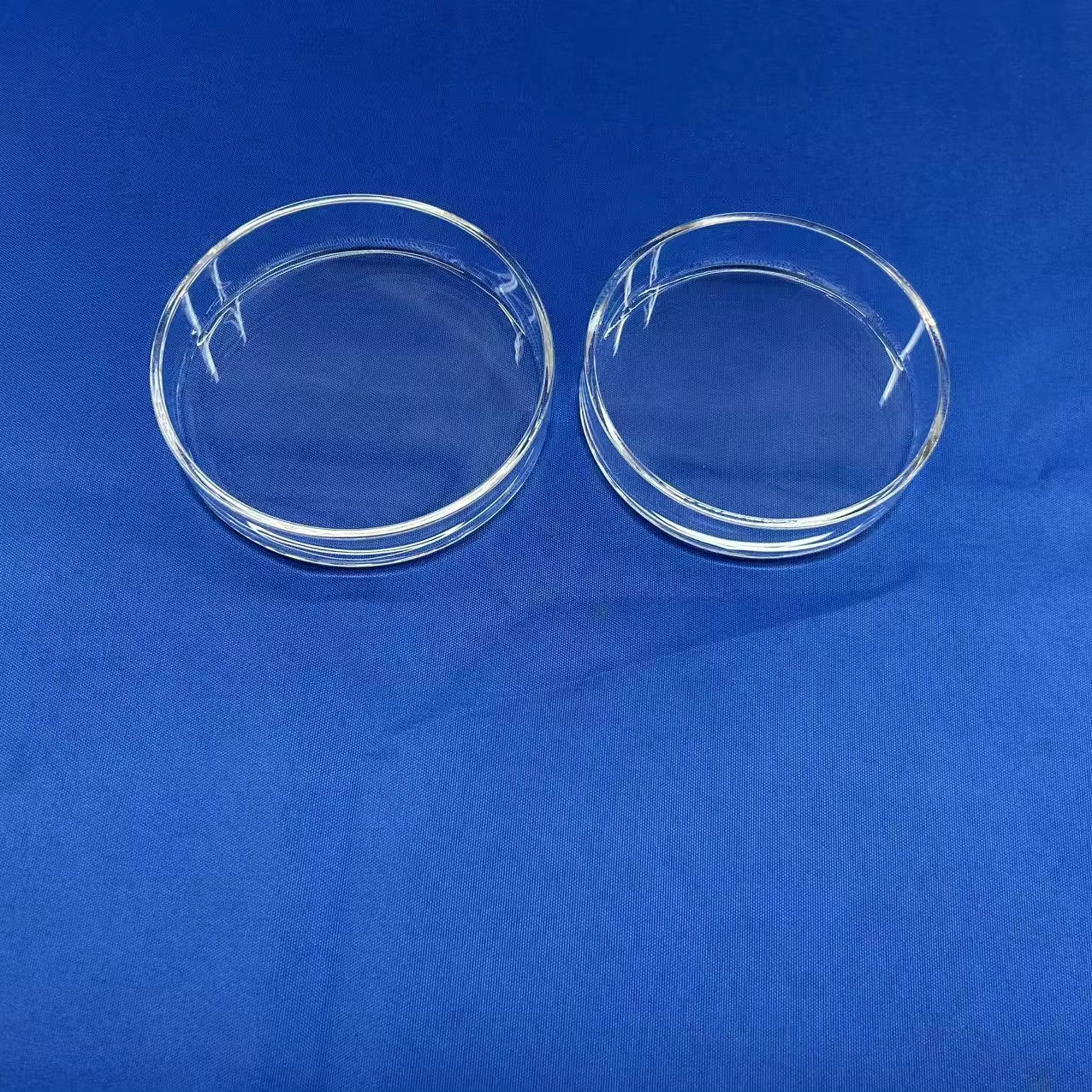
Factory Customized High-purity Quartz Glass Petri Dishes with Lids, for Laboratory, Medical Equipment, Etc.
Flat-bottom chemical-resistant fused silica dishes designed for etching acid handling, thin-film annealing tests, and sterile bio-semiconductor applications. Unaffected by HF immersion alternatives and concentrated mineral acids.
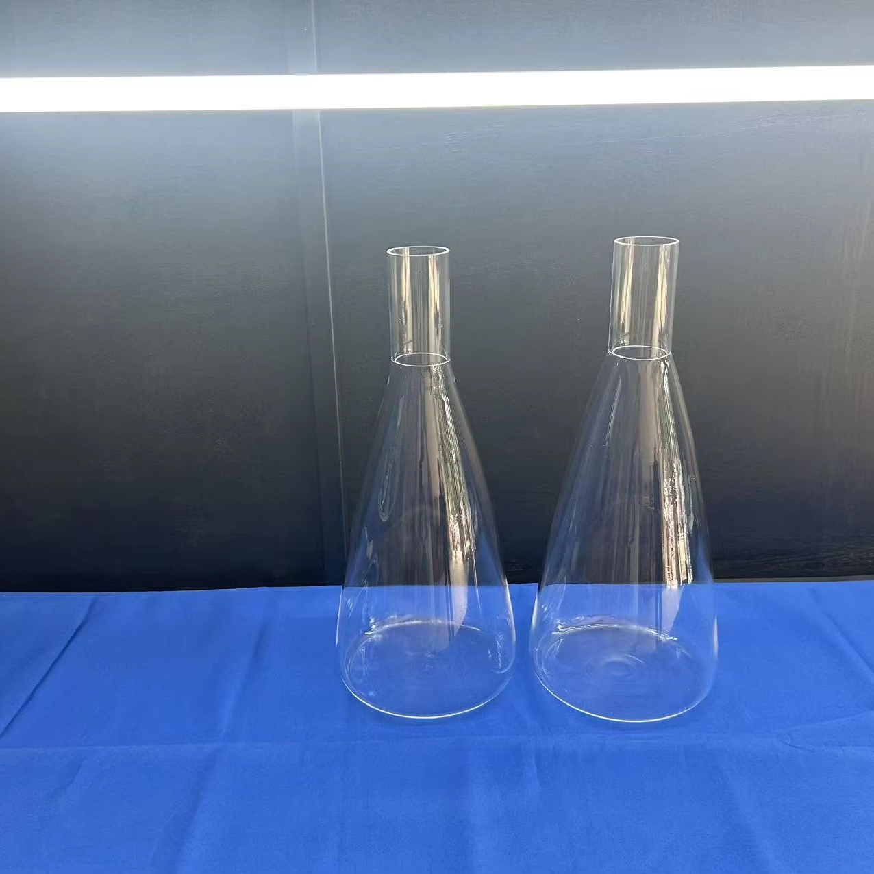
Laboratory Fused Silica Quartz Glass Flask
Round and flat-bottom quartz distillation and reaction flasks capable of withstanding rapid thermal cycling without fracture. Flame-annealed neck joints ensure airtight connections with standard ground taper joints.
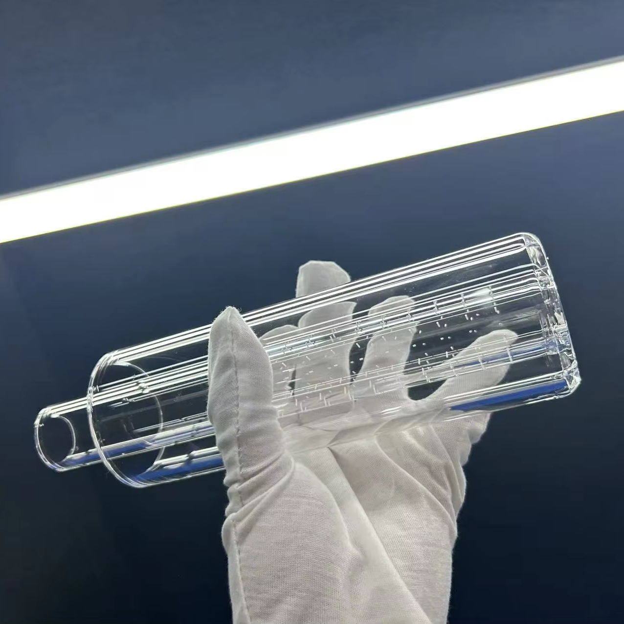
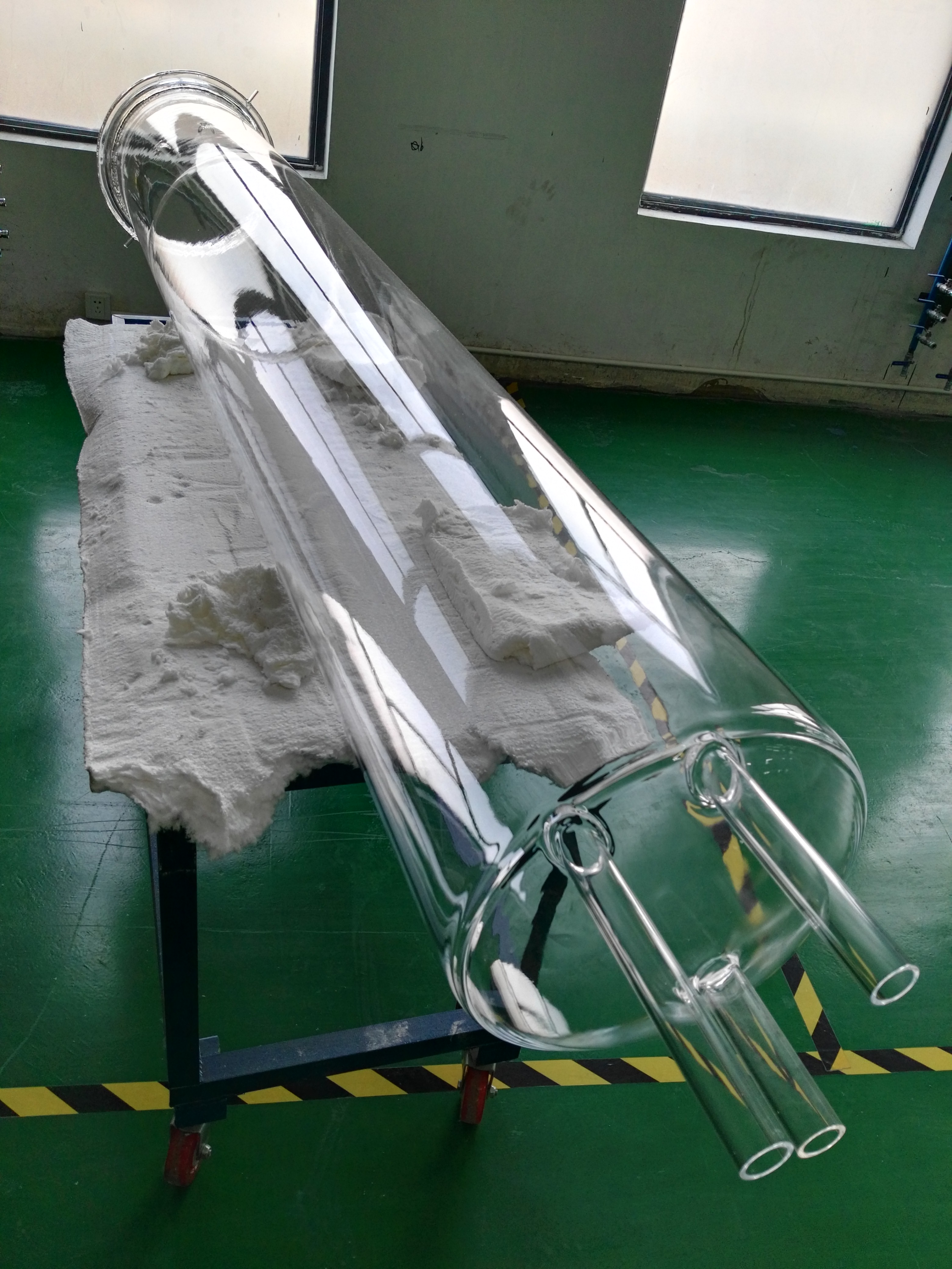
Customized Perforated Quartz Tube
CNC micro-drilled gas distributor tubes engineered for laminar reactive gas distribution in LPCVD and PECVD furnaces. Clean laser-bored perforations preserve mechanical integrity and prevent gas turbulence.
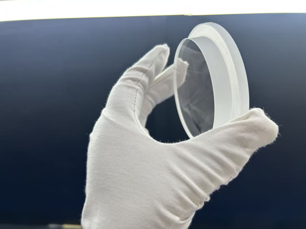
Factory-Made High-purity Ultra-thick Quartz Double-Layer Step Plate ,Provide Cutting and Polishing Services
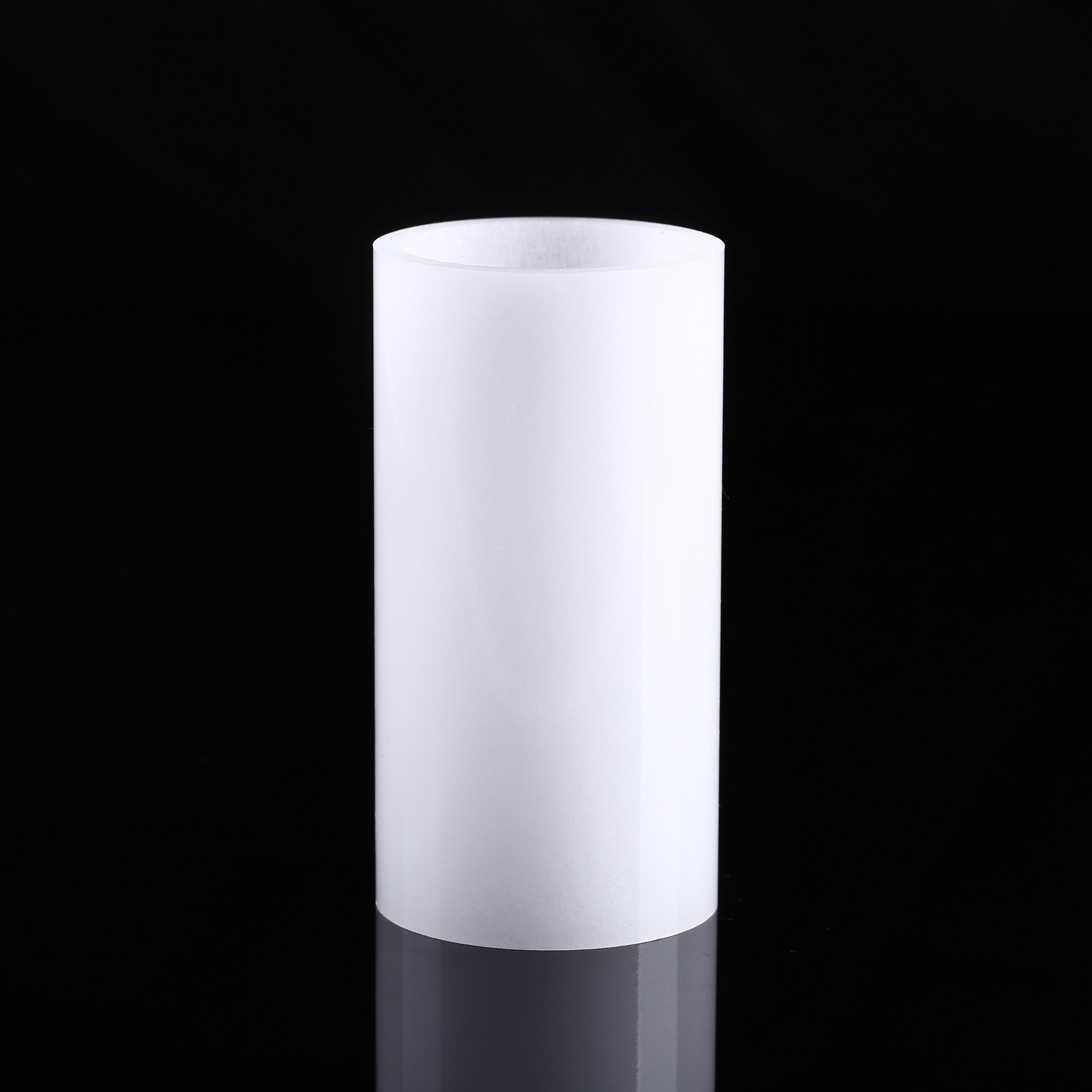
Heavy-gauge double-layer step plates engineered for wafer pedestal supports, RTP susceptors, and vacuum chamber viewports. Optical-grade double-sided chemical mechanical polishing with parallelism within ≤5 arcsec.
High-Purity Fused Silica in Front-End Wafer Fabrication
In modern semiconductor manufacturing, high-temperature thermal processes—such as LPCVD (Low-Pressure Chemical Vapor Deposition), dry/wet thermal oxidation, boron/phosphorus diffusion, and Rapid Thermal Annealing (RTA)—require substrate carrier boats capable of operating continuously between 900°C and 1,250°C. At these extreme thermal budgets, structural materials must exhibit zero chemical volatility, near-zero thermal expansion, and imperceptible trace element leaching.
Donghai County Nivra Quartz Products Co., Ltd. processes premium grade natural quartz crystal sand and synthetic silicon tetrachloride into dimensionally stable, chemically pristine wafer carriers. Our wafer boats eliminate gravitational creep and devitrification phase transformations, providing semiconductor fabs worldwide with a dependable alternative to brittle ceramics and excessively costly CVD-SiC carriers.
Material Property Matrix: Fused Quartz vs. Synthetic Silica vs. CVD Silicon Carbide (SiC)
| Property / Specification Parameter | High-Purity Natural Fused Quartz | Synthetic Fused Silica (JGS1) | Chemical Vapor Deposition SiC |
|---|---|---|---|
| Raw Material Precursor | Donghai Refined Natural Quartz Sand | Vapor-Phase Synthesized SiCl₄ | Silane & Hydrocarbon Precursors |
| Total Metallic Impurities (Fe, Cu, Ni, Na, K) | < 5.0 – 8.0 ppm wt | < 0.1 – 0.5 ppm wt (Sub-ppb class) | < 1.0 – 3.0 ppm wt |
| Hydroxyl (OH⁻) Content | < 5 – 20 ppm (Thermal Grade) | < 1 ppm (Low-OH) or > 1200 ppm (UV) | Non-Hydrated (Zero OH) |
| Softening Point / Maximum Operating Temp | 1,683°C (Continuous at 1,150°C) | 1,600°C (Continuous at 1,100°C) | Decomposes > 2,500°C (Cont. 1,400°C) |
| Coefficient of Thermal Expansion (CTE, 20-300°C) | 5.5 × 10⁻⁷ / °C | 5.0 × 10⁻⁷ / °C | 4.0 × 10⁻⁶ / °C (~8x higher) |
| Thermal Shock Resistance (ΔT Quench) | Excellent (> 1,100°C to ice water) | Exceptional (> 1,150°C to ice water) | Moderate (Prone to thermal shear) |
| HF Acid Cleanability & Surface Reclamation | Controllable Etch Rate (~0.1μm/min in 5% HF) | Uniform Etch Profile without pitting | Impervious (Difficult to chemically strip) |
| Relative Component Acquisition Cost | Cost-Effective Baseline (1.0x) | Moderate Premium (2.2x – 3.0x) | Extreme Capital Investment (6.0x – 10.0x) |
Future Procurement Trends for Semiconductor Quartz Wafer Carriers
Fab managers, equipment OEMs, and global supply chain directors face shifting operational mandates. We identify four primary market forces reshaping fused quartz carrier procurement over the next five years.
1. Accelerated 200mm/300mm Batch Upgrades
With mature-node automotive, power (SiC/GaN), and analog fabs experiencing heavy fab expansions, demand for high-durability 200mm (8") and 300mm (12") horizontal ladder boats is outpacing supply. Procurement teams increasingly secure rolling annual blanket contracts with verified direct manufacturers to buffer against lead-time volatility.
2. Stringent Sub-ppb Alkali Metal Limits
Trace mobile ions, especially Sodium (Na+) and Potassium (K+), induce gate oxide breakdown and threshold voltage shifts in sub-7nm and 3D NAND memory processes. Sourcing specifications now mandate verified ICP-MS spectral analysis below 0.1 ppm total metals, with synthetic quartz liners reserved for the most critical front-end device layers.
3. Monolithic Laser Slotting over Manual Welding
Traditional hand-assembled cross-rod boats are being phased out by Tier-1 automated fabs. Modern robotic end-effectors require slot pitch position accuracy within ±0.02 mm. CNC 5-axis ultrasonic and diamond laser-slotted monolithic quartz rails eliminate human welding variances, reducing notch stress concentrations and particulate shedding.
4. Supply Chain Direct-Sourcing from Donghai
Semiconductor procurement directors are bypassing multi-layer trading intermediaries to partner directly with primary Chinese processing factories in Donghai County. Direct engagement reduces piece prices by 25% to 40%, provides unfiltered engineer-to-engineer drawing reviews, and guarantees customized traceability documentation.
Engineering Advancements in Quartz Wafer Carrier Fabrication
Eliminating robotic wafer transfer errors and catastrophic thermal devitrification demands specialized glass-working discipline. Discover the four core engineering milestones mastered in our cleanroom facilities.
Sub-Micron CNC Laser & Diamond Profiling
Wafer carriers must guarantee precise substrate parallel alignment under high gas flow velocities. We employ multi-axis high-speed CNC cutting centers equipped with chilled diamond profiling wheels and pulsed laser cutters to maintain wafer slot width tolerances of ±0.03 mm and cumulative pitch tolerances within ±0.05 mm across 1,000 mm lengths.
Inert Gas-Shielded H₂/O₂ Micro-Flame Fusion
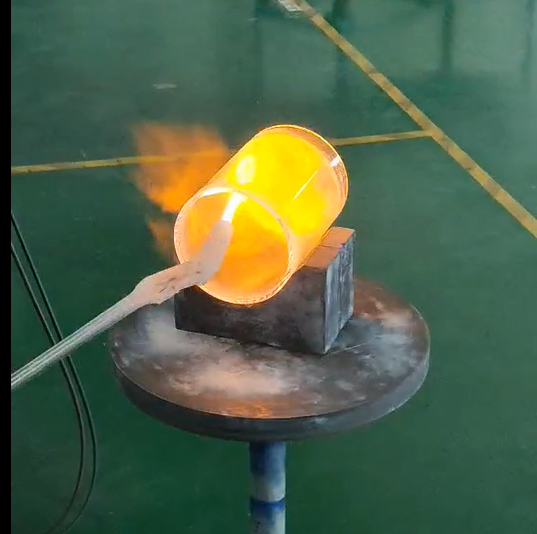
Conventional glassblowing introduces trapped micro-bubbles and hydroxyl (OH−) precursors at joint interfaces. Nivra employs specialized hydrogen-oxygen micro-torches enveloped in high-purity argon (Ar) shielding. This technique preserves continuous molecular amorphous SiO₂ lattice structures, avoiding brittle notch cracking under repeated thermal cycling.
Controlled Annealing & Polarimetric Inspection
Thermal stresses generated during cutting and torch welding are completely eliminated through our multi-stage clean electric annealing kilns at 1,150°C, followed by programmed ramp-down rates (<1.5°C/min). Residual birefringence is monitored using dual-wavelength optical polariscopes to verify internal stress levels ≤ 10 nm/cm.
Donghai County Nivra Quartz: Manufacturing Authority
Established in February 2019 in Donghai County, Jiangsu—China's crystal capital—Nivra operates a certified integrated fabrication complex dedicated to high-performance fused quartz components.
Integrated Supply Chain at the Silicon Source
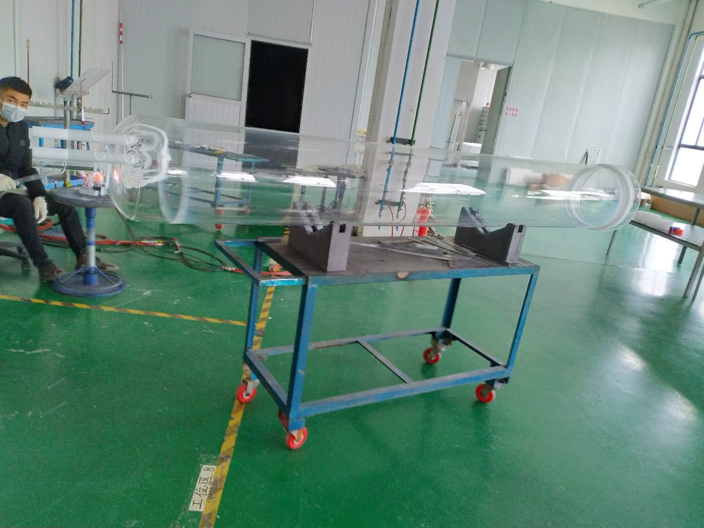
Located at 285 Heping East Road, Lianyungang, Jiangsu, Nivra leverages primary access to China's purest silica deposits. Our production facilities encompass every phase of quartz manipulation: raw ingot slicing, CNC core drilling, high-precision surface grinding, laser micro-slotted machining, cleanroom chemical etching, and optical double-sided polishing.
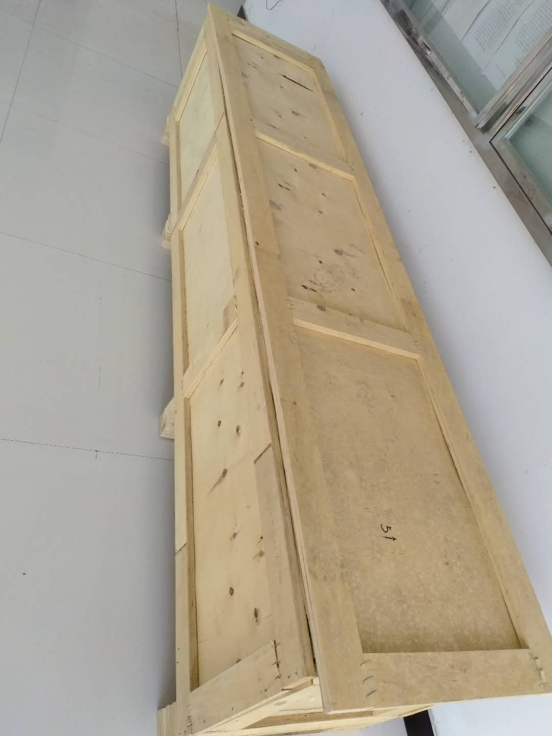
Overseas semiconductor fabs and research institutes face severe risks from transit breakage and sub-standard packaging. Every Nivra quartz carrier is cleaned with Class 10 cleanroom UPW (>18.2 MΩ·cm), vacuum sealed in anti-static PE film, suspended inside custom molded EPE shock-absorbent cassettes, and secured in international fumigation-free wooden export crates.
 Precision Machining & Cutting
 Flame Fusion & Annealing
 CMM Inspection & Cleaning
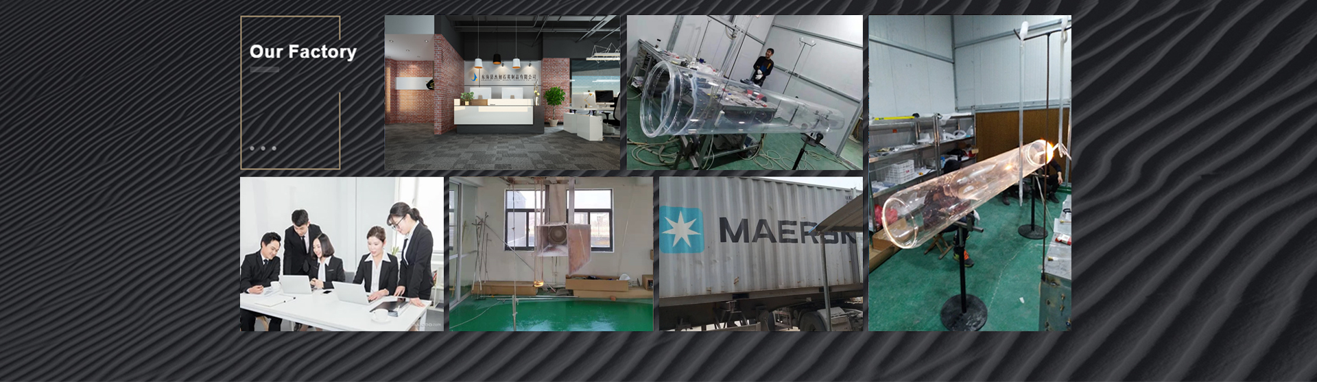
 Donghai Facility Workshop
Audited Production Compliance & Qualification Documents
Frequently Asked Questions for Fab Procurement & Engineers
Technical insights addressing furnace lifetime optimization, devitrification kinetics, chemical cleaning bath chemistries, and custom CAD drawing requirements.
What causes devitrification in quartz wafer boats, and how does Nivra Quartz prevent premature crystallization? +
Devitrification is the phase transformation of metastable vitreous (amorphous) silica into crystalline β-cristobalite occurring between 1,150°C and 1,300°C. Upon subsequent cooling below 270°C, cristobalite undergoes an abrupt α–β displacive structural inversion accompanied by a 5% volume contraction, triggering microscopic surface crazing, white hazing, and eventual structural rupture.
Devitrification is catalyzed by surface alkaline contamination (Na, K, Ca) and water vapor. Nivra mitigates this by: (1) using raw quartz sand with alkali content < 0.1 ppm; (2) applying deep HF acid-etch pickling to remove microscopic micro-cracks and nucleation sites; and (3) executing fire-polishing across all CNC-machined slot faces to produce an atomically smooth, sealed vitreous barrier.
What dimensional tolerances can you hold for automated robotic end-effector wafer transfer systems? +
Automated wafer handlers, vacuum cassette elevators, and robotic transfer arms demand exceptionally tight physical interfaces to prevent substrate dropping, edge scratching, or cassette collision alarms.
For 150mm, 200mm, and 300mm wafer carriers, Nivra guarantees individual slot pitch tolerances within ±0.02 mm, cumulative pitch variation within ±0.05 mm across entire furnace lengths, slot tilt parallelism < 0.05°, and total carrier camber / twist under 0.15 mm. All measurements are certified using 3D Coordinate Measuring Machines (CMM) and non-contact laser optical profilers before shipment.
How does fused quartz compare against CVD Silicon Carbide (SiC) for high-temperature diffusion carriers? +
While CVD-SiC provides exceptional stiffness and resists gravitational sag above 1,300°C, it exhibits significant drawbacks: (1) an acquisition cost 6x to 10x higher than fused quartz; (2) extreme mechanical brittleness, making accidental handling impact catastrophically expensive; and (3) severe difficulties in chemical stripping of heavy LPCVD dielectric deposits.
High-purity fused quartz remains the global workhorse material for processes up to 1,200°C. It offers a near-zero CTE (5.5 × 10⁻⁷/°C) ensuring immunity to thermal shock cracking, easy wet-chemical etching reclamation in standard HF baths, and far superior total cost of ownership (TCO).
What is the recommended acid cleaning protocol to maximize the operating lifespan of quartz wafer boats? +
To strip CVD nitride, oxide, or poly-Si films without excessively etching the quartz substrate, fabs should utilize a 5% to 10% hydrofluoric (HF) acid bath mixed with nitric acid (HNO₃) to dissolve metallic impurities. Immersion durations should not exceed 10 to 15 minutes, with bath temperatures maintained below 30°C to prevent excessive dimensional loss.
Following chemical stripping, carriers must be rinsed in cascade overflow DI water until effluent resistivity reaches 18 MΩ·cm, followed by cleanroom nitrogen drying and furnace bake-out at 800°C to bake off volatile fluorides before returning to active production.
Can you produce custom quartz boats directly from customer CAD drawings (STEP, DWG, DXF)? +
Yes. Over 70% of our production volume comprises fully customized OEM/ODM builds tailored to proprietary furnace fixtures (including ASM, TEL, Kokusai, and Baccini platforms).
Customers can send 2D PDFs with critical tolerances and 3D CAD files (STEP, IGES, DWG, DXF). Our design engineers conduct complete Design for Manufacturability (DFM) reviews—confirming slot widths, rod diameter selections, expansion relief gaps, and flame-torch clearances—and provide a comprehensive engineering feedback report within 5 hours.
What are the minimum order quantities (MOQ) and production lead times for standard vs. custom quartz carriers? +
We maintain highly flexible procurement structures:
Prototype & Sample Validation: MOQ is 1 piece for custom wafer boats and large-diameter diffusion components. Lead time is typically 7 to 12 working days.
Volume Production Runs: 10 to 500+ pieces, with delivery staggered according to your fab’s monthly pull schedules. Standard replacement parts and bare fused quartz tubes/plates ship within 3 to 5 business days from our bonded finished-goods inventory.
What packaging protocols are implemented to prevent transit micro-fractures during air and ocean freight? +
High-aspect-ratio ladder boats are inherently fragile when subjected to transport harmonic vibrations and drop acceleration forces.
Every carrier undergoes cleanroom ultrasonic degreasing, double-layer anti-static heat sealing, and encapsulation inside custom CNC-cut high-density expanded polyethylene (EPE) foam nests. These internal modules are suspended in shock-isolated heavy-gauge inner boxes, then enclosed in IPPC-certified fumigation-free plywood export crates equipped with external tip-and-tilt and drop-impact recording indicators.
What optical and purity certificates are supplied with each production batch? +
Every production lot ships with a comprehensive Quality Inspection Dossier, including:
1. Certificate of Analysis (COA): ICP-MS glow-discharge spectrometry data detailing trace elements (Fe, Al, Cu, Mg, Ti, Ca, Na, K, Li).
2. CMM Dimensional Inspection Report: Point-to-point verification of critical slot pitches, overall length, perpendicularity, and tooth depths.
3. Polariscope Stress Verification: Certification of internal optical birefringence below 10 nm/cm.
4. Material Origin Traceability: Conformance to international RoHS, REACH, and SEMI material standards.
Request an Engineering Review & Direct Factory Quotation
Connect directly with our technical team in Donghai County. Send your wafer boat CAD drawings, slot specifications, or furnace tube bill-of-materials for immediate analysis.