Featured Precision Fused Quartz & Silica Products
Standard and custom-engineered quartz components manufactured with high chemical purity, exceptional thermal resistance, and tight dimensional tolerances for global industrial and lab environments.
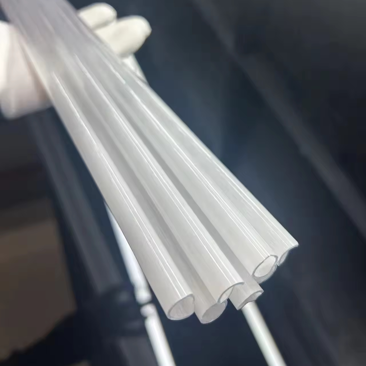
Translucent Quartz Glass Pipe Quartz Glass Sleeve Opaque Milky White Quartz Glass Tube
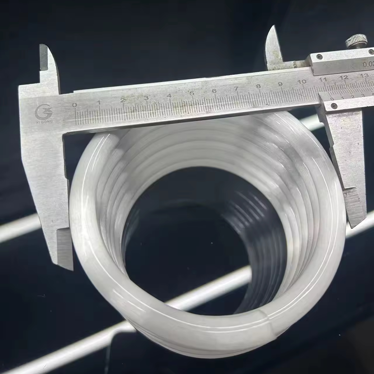
Helical Clear Quartz Glass Coil t Tube
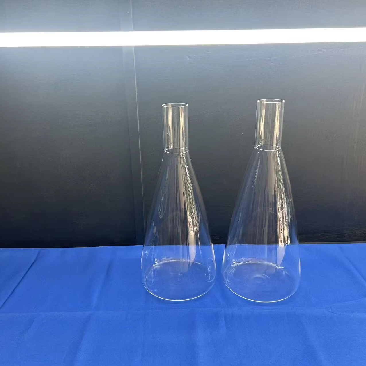
Laboratory Fused Silica Quartz Glass Flask
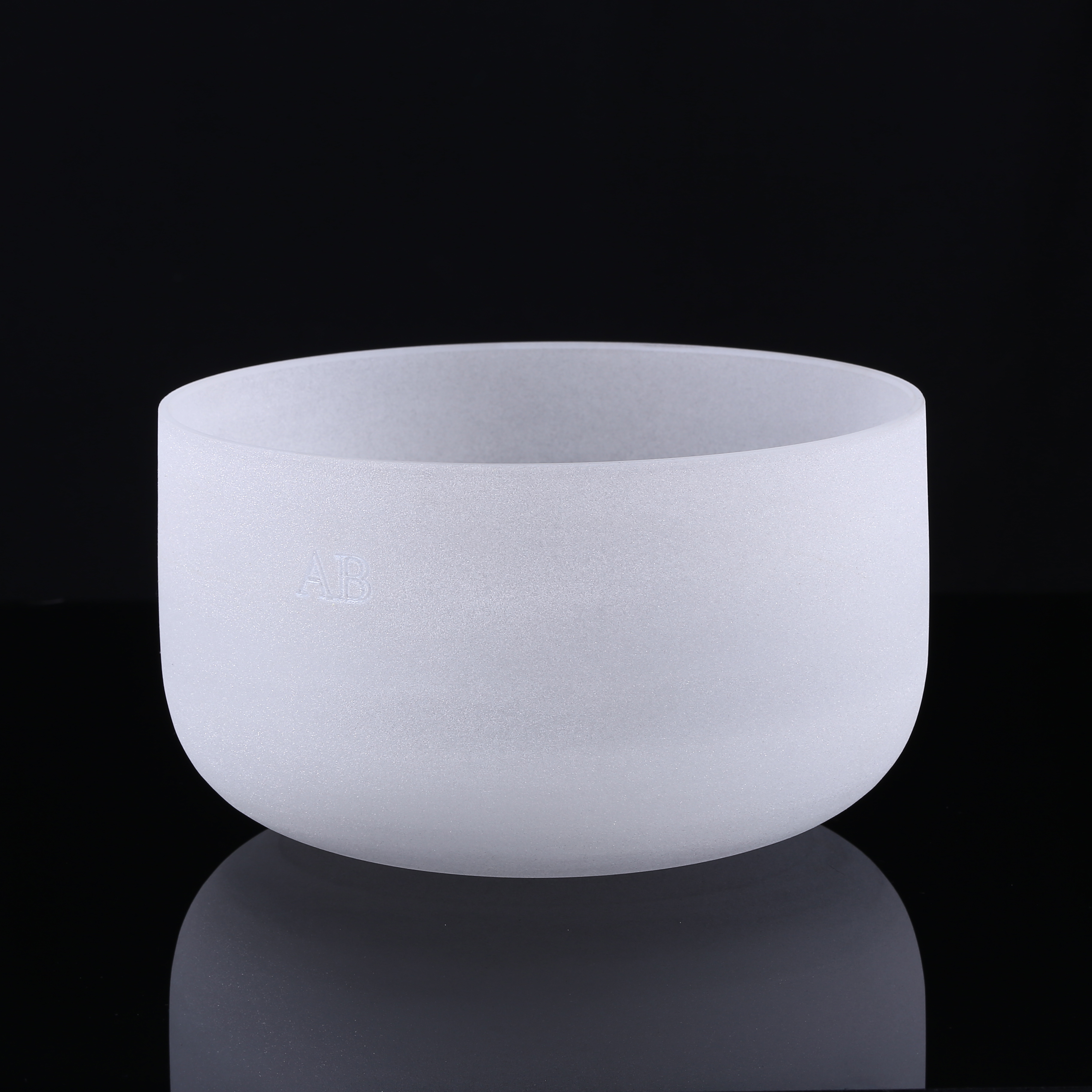
High Temperature Fused Silica Quartz Crucible
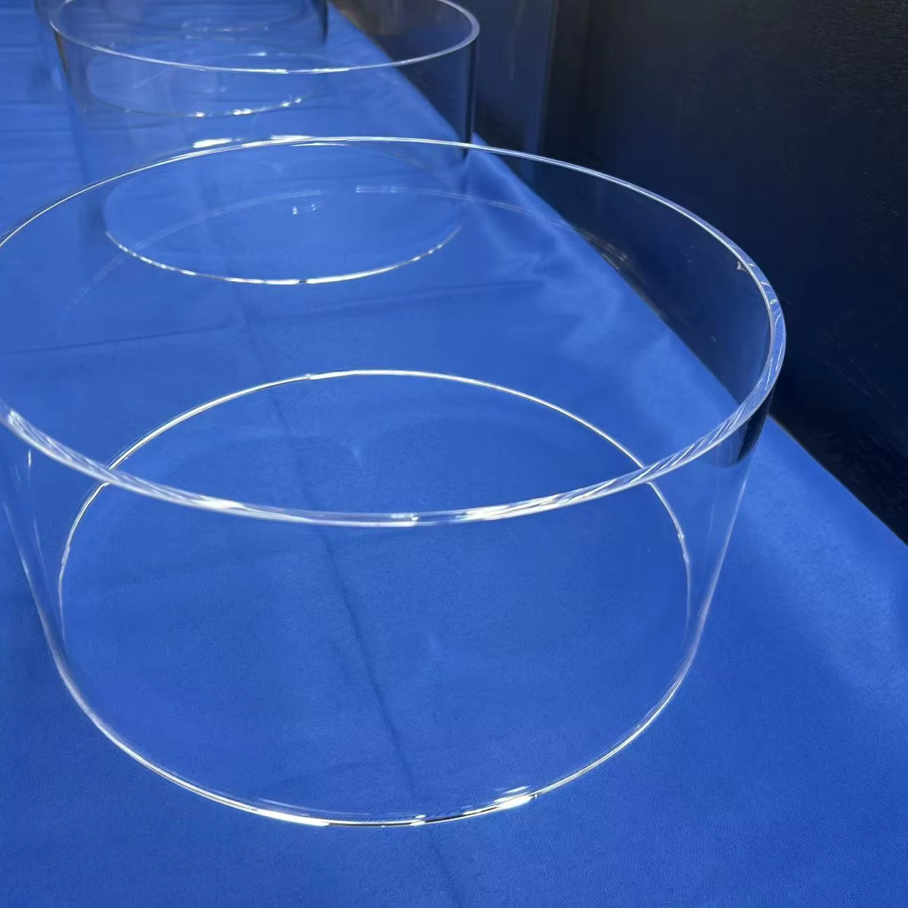
High-Purity Fused Quartz Large Diameter Round Rods Cutting Welding & Bending Services ForIndustrial Production
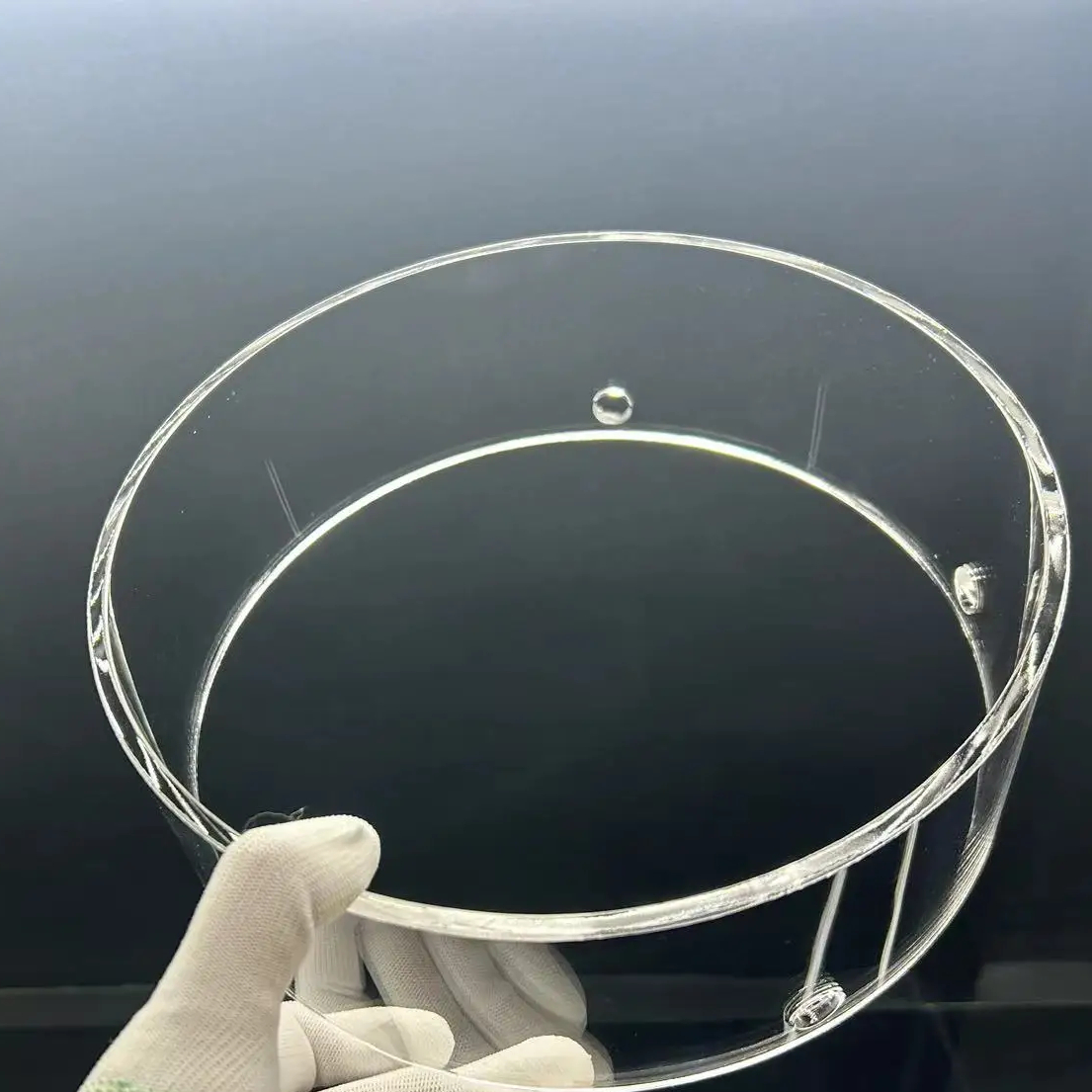
Fused Transparent Quartz Tube
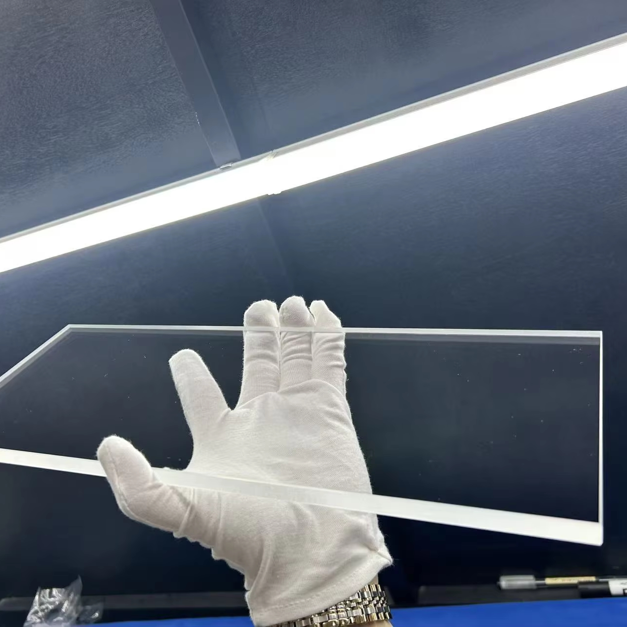
Ultra Clear High Purity Quartz Sheet
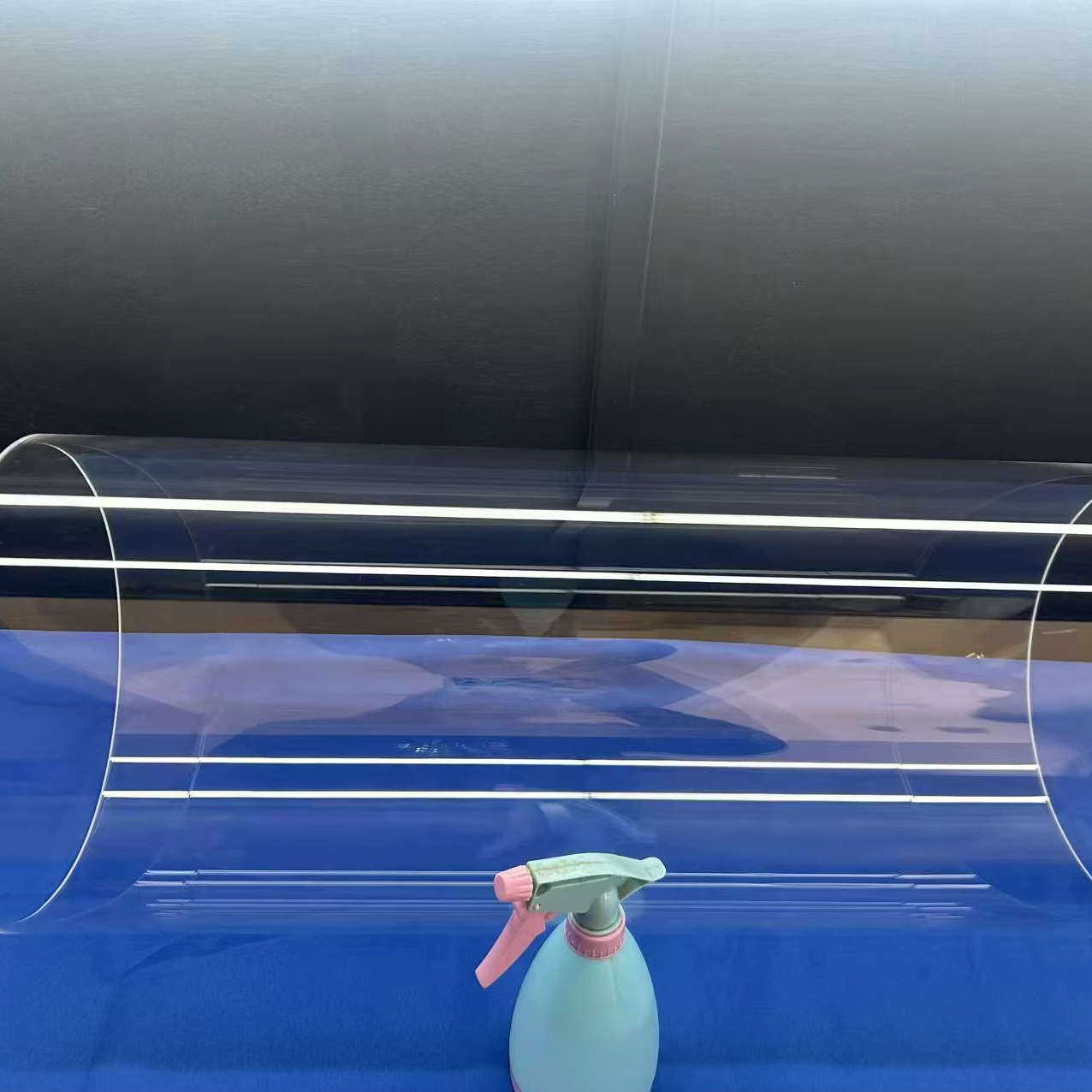
Customizable High Purity Fused Quartz Glass Tube High Temperature Resistant
How Engineering Teams Benchmark Fused Silica Manufacturers
Specifying optical-grade quartz plates requires evaluating precise thermodynamic, chemical, and optical parameters to prevent optical distortion, thermal fracturing, and plasma degradation.
Hydroxyl (OH⁻) Content
Determines optical transmission windows. High OH (>1000 ppm) provides superior deep-UV transmission (185–260 nm), while Low OH (<1–5 ppm) eliminates the 2.73 µm absorption dip for critical near-IR performance.
Thermal Shock Stability
A remarkably low coefficient of thermal expansion (CTE ≈ 5.5 × 10⁻⁷ /°C) enables rapid thermal cycling from 1100°C continuous operation down to ambient water quenching without structural stress fracture.
Bubble Class & Inclusions
Classified strictly according to DIN 58927 / ISO 12123 standards. Precision lithography and laser windows mandate Bubble Class 0 (zero discernible bubbles >0.05 mm) to avoid beam deflection and laser damage.
Chemical Purity (ppb Level)
Trace metallic impurities (Al, Fe, Ti, Na, K, Li) must remain below 10 ppm total for industrial furnace grades and below 10 ppb for semiconductor wafer processing to ensure zero ionic cross-contamination.
Top 10 Fused Silica Plate Manufacturers & Factories
An independent industry benchmark analyzing global primary producers, optical fabricators, and regional quartz clusters supplying semiconductor, aerospace, and precision optical industries.
Donghai County Nivra Quartz Products Co., Ltd.
Positioned at the epicenter of the world's crystal and natural silica processing hub, Nivra Quartz integrates high-purity ingot fusion with end-to-end CNC machining, optical wafer lapping, double-sided chemical mechanical planarization (CMP), and flame craftsmanship. Serving semiconductor wafer carrier, laser optical window, and industrial furnace buyers across North America (40%) and Europe (34%), Nivra provides factory-direct custom fabrication directly against CAD/STEP drawings with an audited 5-hour engineering turnaround.
Heraeus Conamic
Global benchmark in synthetic fused silica (Suprasil®) and high-purity natural quartz (Spectrosil®). Specializes in extreme-UV lithography optics, telecommunication preforms, and high-temperature wafer carrier plates with ultra-low trace element concentration.
Corning Incorporated
Known for HPFS® (High Purity Fused Silica) 7980, 7979, and ULE® titania-doped zero-expansion silica. Offers market-leading refractive index homogeneity, high laser damage thresholds, and world-class transmission for aerospace and excimer laser plates.
Tosoh Quartz Corporation
A key subsidiary of Tosoh Corporation, delivering precision-fabricated fused quartzware for Japanese and global semiconductor fabrication plants. Renowned for dry-etching rings, large diffusion plates, and synthetic photomask substrates with tight particle controls.
Momentive Technologies
Formerly GE Quartz, Momentive manufactures industry-standard Type 214 and Type 124 fused quartz materials. Highly regarded for thermal sag resistance, high electrical breakdown strength, and consistency across large-diameter fused quartz discs and plates.
Shin-Etsu Chemical Co.
World leader in synthetic quartz ingots synthesized via the vapor-phase axial deposition (VAD) technique. Supplies zero-defect photomask plates, LCD stepper projection windows, and advanced laser optics characterized by extreme radiation resistance.
Saint-Gobain Quartz
A heritage European manufacturer recognized for Quartzel® fibers and specialty thermal fused silica plates. Provides engineered solutions for high-energy physics, thermal insulation shields, and specialized optical instrumentation plates for aggressive environments.
QSil GmbH
Specializes in electric-fused and plasma-melted fused quartz ingots, hollow cylinders, and thick-slab optical plates. Focuses heavily on high-temperature resistance, photovoltaic crucible precursors, and UV-transmissive analytical observation plates.
Hubei Feilihua Quartz Glass
The first Chinese quartz glass manufacturer certified by international semiconductor equipment fabricators (TEL, Lam). Produces large-scale synthetic fused silica blocks, aerospace radome plates, and high-purity optical blanks with advanced laser verification.
CoorsTek Inc.
Advanced technical ceramics and glass titan delivering high-performance opaque and transparent silica plates. Dominates semiconductor wafer-handling end effectors, dielectric insulation shields, and chemically inert analytical chamber windows.
Optical & Physical Grade Comparison: JGS1, JGS2 & JGS3
Ensure you select the exact optical grade required for your transmission spectrum without over-specifying raw material cost or sacrificing ultraviolet and infrared performance.
| Grade Type | Primary Synthesis Method | Transmission Range | OH⁻ Content | Refractive Index (nd) | Primary Application Areas |
|---|---|---|---|---|---|
| JGS1 (Far UV) | Synthetic SiCl₄ Flame Hydrolysis | 185 nm – 2500 nm | > 1200 ppm | 1.4585 | Deep-UV lasers, excimer lithography windows, analytical cuvettes |
| JGS2 (UV-Vis) | Refined Natural Quartz Gas Fusion | 220 nm – 2500 nm | 100 – 200 ppm | 1.4585 | Optical observation windows, sight glasses, UV disinfection shields |
| JGS3 (Infrared) | Electrically Vacuum Fused Silica | 260 nm – 3500 nm | < 5 ppm | 1.4584 | IR pyrometry windows, thermal vision sensors, low-OH heaters |
| Opaque Silica | Electric Arc Sintered Natural Silica | Scattered / Diffuse | Variable | N/A | Heat shields, furnace door thermal plugs, semiconductor baffles |
| Sapphire (Al₂O₃) | Kyropoulos Single Crystal Growth | 200 nm – 5000 nm | None | 1.768 | Extreme scratch resistance, extreme pressure sight windows |
Future Sourcing & Technological Trends (2025–2030)
Strategic shifts in semiconductor nodes, laser manufacturing, and global raw material refinement are changing how fused silica plates are specified, priced, and sourced.
Sub-2nm Lithography Cleanliness
As semiconductor fabrication moves toward Angstrom-level nodes and high-NA EUV lithography, quartz plate cleanliness standards are transitioning from parts-per-million (ppm) to sub-parts-per-billion (ppb). Surface defect thresholds now strictly demand zero micro-scratching (<10/5 scratch-dig) and complete elimination of mobile ionic contaminants like Na+ and K+ that degrade wafer yields.
Large-Format Substrate Scaling
High-power industrial fiber laser cutting heads (>30 kW) and Gen 10.5 display manufacturing require ultra-large continuous quartz plate formats exceeding 600 mm × 600 mm with wave-front distortion below λ/4 across the entire clear aperture. Fabricators capable of cold-processing monolithic large-format blanks without inducing internal mechanical birefringence hold strong market pricing power.
The Donghai Cluster Hub Advantage
Global supply chains are consolidating procurement within the Donghai quartz industrial cluster. By combining direct access to high-purity natural silica reserves with integrated high-speed CNC multi-axis machining, ultrasonic boring, and rapid flame-annealing facilities, modern Donghai fabricators like Nivra Quartz achieve a 30–45% lead-time reduction over Western legacy suppliers, accompanied by responsive engineering agility.
Inside Precision Cold & Hot Glass Fabrication
Transforming fused silica ingots into optical-grade plates and complex semiconductor quartzware requires a multi-stage production chain under cleanroom conditions.
1. Diamond Wire Slicing
High-precision multi-wire diamond saws slice fused silica ingots into wafer blanks with minimal kerf loss and sub-0.05 mm thickness variation, ensuring stress-free parallel surfaces.
2. Double-Sided Lapping
Planetary double-sided lapping machines use fine cerium oxide and diamond abrasives to progressively reduce micro-roughness, achieving strict flatness and parallelism (<3 arcseconds).
3. Chemical Planarization (CMP)
Sub-surface damage (SSD) is completely removed through chemical mechanical polishing, attaining laser-ready optical finishes with surface roughness Ra < 0.5 nm and scratch-dig 20/10.
4. Zygo Laser Interferometry
Every finished optical plate is verified on Zygo He-Ne laser interferometers and spectrophotometers to generate certified transmission curves and transmitted wavefront error documentation.
Why Engineering Procurement Teams Rely on Nivra Quartz
Located at 285 Heping East Road, Lianyungang, Jiangsu, Nivra Quartz combines large-scale manufacturing discipline with rapid engineering customization.
Integrated Production Base
Staffed by 101–200 skilled operators and engineers, our facility encompasses over 5,000 square meters of dedicated cold cutting, ultrasonic CNC milling, cleanroom double-sided polishing, flame lathe fire-working, and strict QA laboratories.
Sub-5-Hour Engineering Feedback
We maintain an audited 88.89% inquiry response rate with engineering feedback delivered within 5 hours. Experienced quartz fabrication specialists review your tolerance drawings, chamfer details, and thermal operating environments directly.
Breakage-Proof Export Crating
Shipping precision glass globally requires specialized protective engineering. Every quartz plate is ultrasonically cleaned, individually sealed in multi-layer vacuum foil, encased in shock-absorbing high-density polyethylene foam, and secured in export-grade fumigation-free wooden crates.
Frequently Asked Questions: Fused Silica Procurement
Authoritative answers to common technical queries submitted by optical engineers, semiconductor toolmakers, and procurement directors.
What is the fundamental difference between fused quartz and synthetic fused silica plates?
Fused quartz is produced by electrically melting or flame-fusing naturally occurring high-purity crystalline quartz sand (SiO₂ > 99.99%). It offers superior thermal stability, low thermal expansion, and exceptional cost efficiency for furnace tubes, crucibles, and general optical plates. Synthetic fused silica is created chemically through the vapor-phase flame hydrolysis of silicon tetrachloride (SiCl₄), achieving extreme chemical purity (> 99.9999%), virtual absence of metallic impurities, zero bubble content, and high deep-UV transmission down to 185 nm (JGS1 grade).
How does the OH⁻ (hydroxyl) radical affect plate transmission in the infrared spectrum?
Hydroxyl ions (OH⁻) incorporated within the amorphous SiO₂ matrix produce fundamental vibrational absorption bands at 2.73 µm, with harmonic overtones at 2.22 µm and 1.38 µm. For infrared pyrometry, NIR laser optics, or optical sensing between 2500 nm and 3500 nm, low-OH fused silica (JGS3 / IR grade) with < 5 ppm OH⁻ must be specified to eliminate transmission dips and prevent thermal optical distortion.
What mechanical tolerances and surface flatness can Nivra Quartz achieve for custom plates?
For custom optical plates, round sight discs, and rectangular substrates, standard dimensional tolerances can be held to ±0.05 mm, with precision CNC ground steps, drilled holes, and waterjet bevels. Optically polished surfaces achieve flatness up to λ/10 per inch @ 632.8 nm, parallelism < 5 arcseconds, surface roughness Ra < 0.5 nm, and MIL-PRF-13830B scratch-dig quality of 20/10 or 40/20 depending on requirements.
What is the continuous vs. short-term operating temperature threshold for fused silica plates?
Clear fused silica and quartz plates can operate continuously at approximately 1100°C in air and inert environments. Short-term exposure limits reach 1450°C. The transformation point occurs at approximately 1075°C, the annealing point at 1180°C, and the softening point at 1683°C. When operating near or above 1150°C, plates must not be held indefinitely in contact with alkali dust or finger oils, which catalyze surface devitrification (recrystallization into cristobalite).
What are the standard Minimum Order Quantities (MOQ) and prototype delivery schedules?
We maintain low MOQ thresholds to support research and development: standard dimension plates and prototypes start from 1 to 10 pieces, while high-volume semiconductor disc runs begin at 50 to 100 pieces. Rapid prototypes for non-standard thicknesses or custom geometries typically ship within 7 to 10 business days following CAD confirmation, accompanied by full dimensional inspection reports.
Can Nivra Quartz provide specialized edge treatments, stepped lips, and custom cutouts?
Yes. We specialize in custom CNC 4-axis profile grinding. We routinely fabricate circular stepped sight glasses with O-ring sealing grooves, counter-bored mounting holes, chamfered edge bevels (45° or custom radius to eliminate stress risers), fire-polished rounded safety edges, and laser-etched fiducial marks or part serialization numbers for traceability.
Accelerate Your Quartz Sourcing Project Today
Whether you need custom-dimensioned JGS1 optical windows, high-temperature furnace sight plates, or precision semiconductor boats and flanges, our engineering team in Donghai provides fast CAD reviews, sample prototypes, and volume quotations.
Get Catalog