Precision Fused Quartz Components & Assembly Series
Explore our core engineering product portfolio manufactured in Donghai, China. Custom sizes, optical polishing, flame treatments, and special hole drilling available upon request.
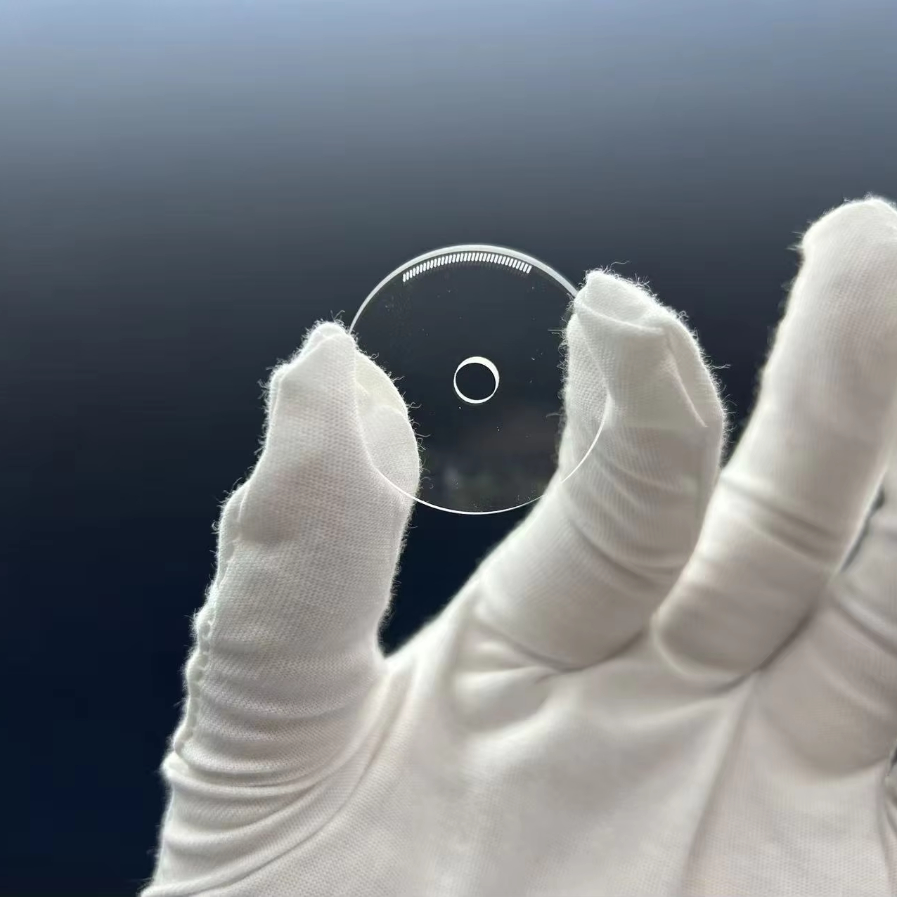
Frosted Quartz Sheet
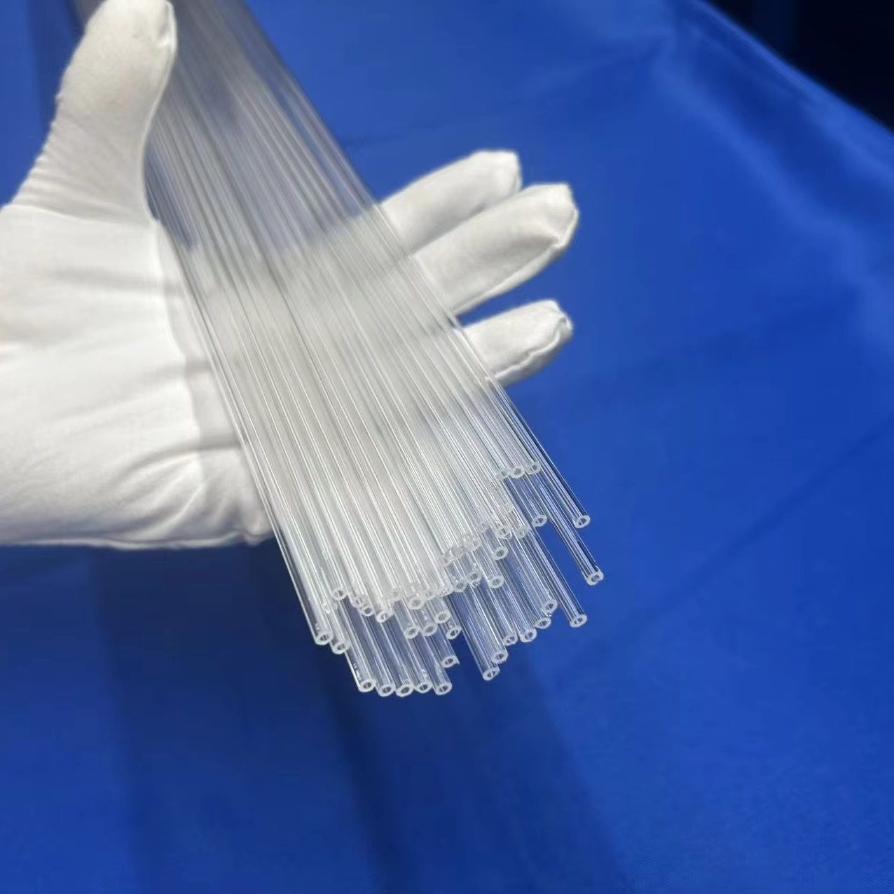
Capillary Quartz Tube
High-Purity Fused Quartz Rods Cutting & Bending
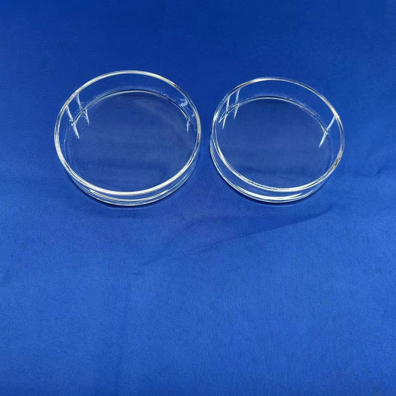
Quartz Glass Petri Dishes with Lids
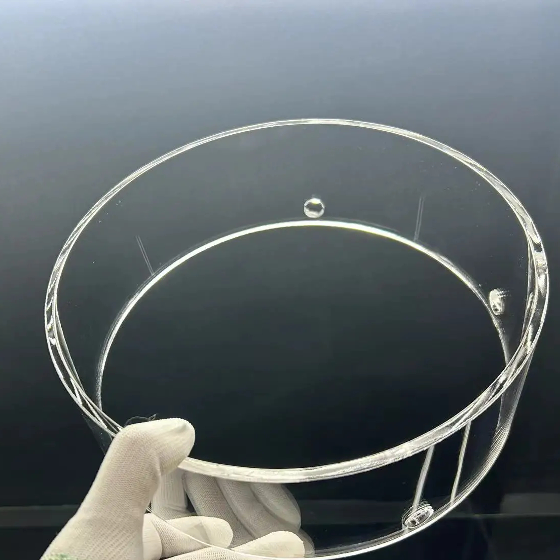
Fused Transparent Quartz Tube
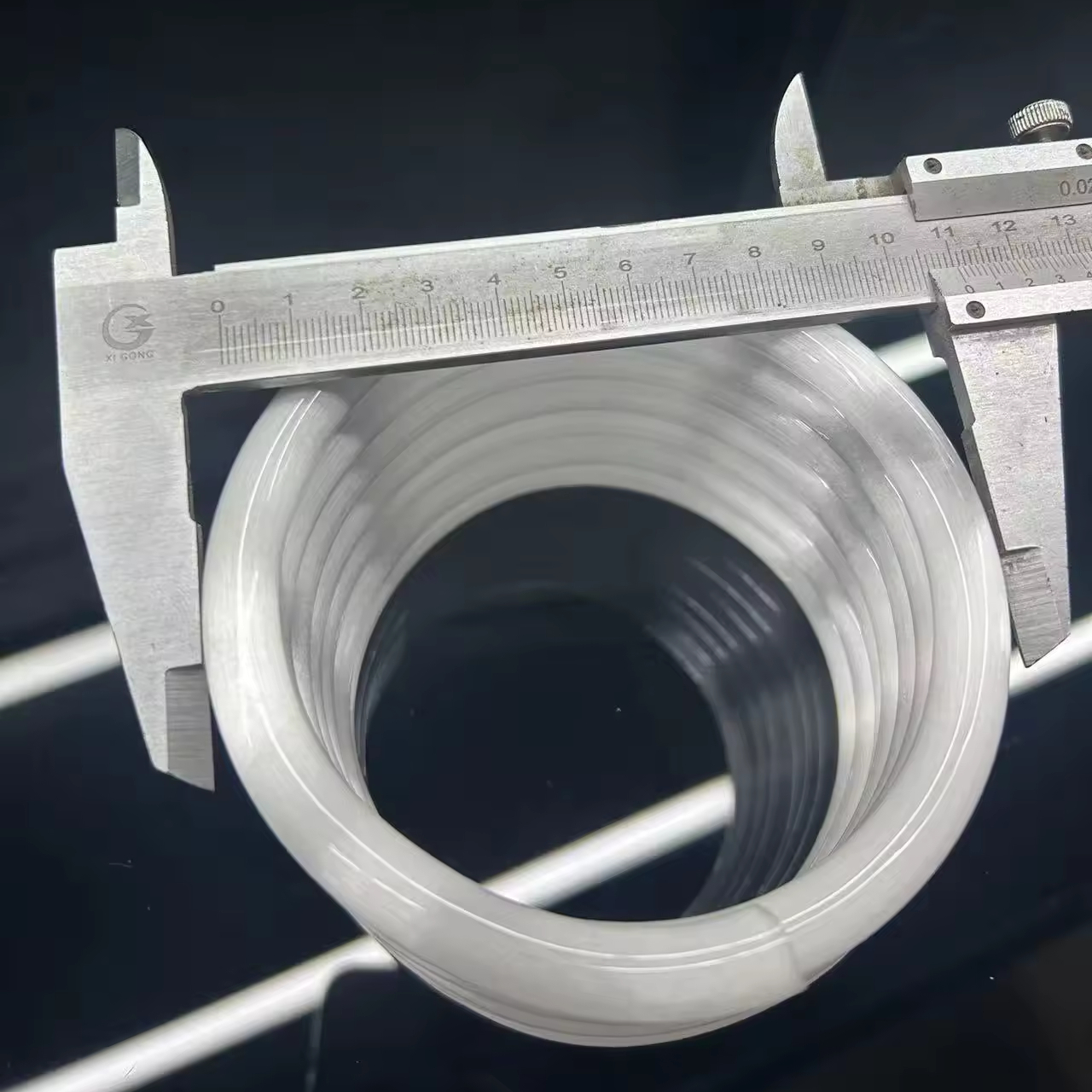
Helical Clear Quartz Glass Coil Tube
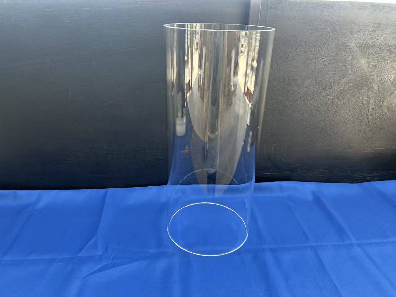
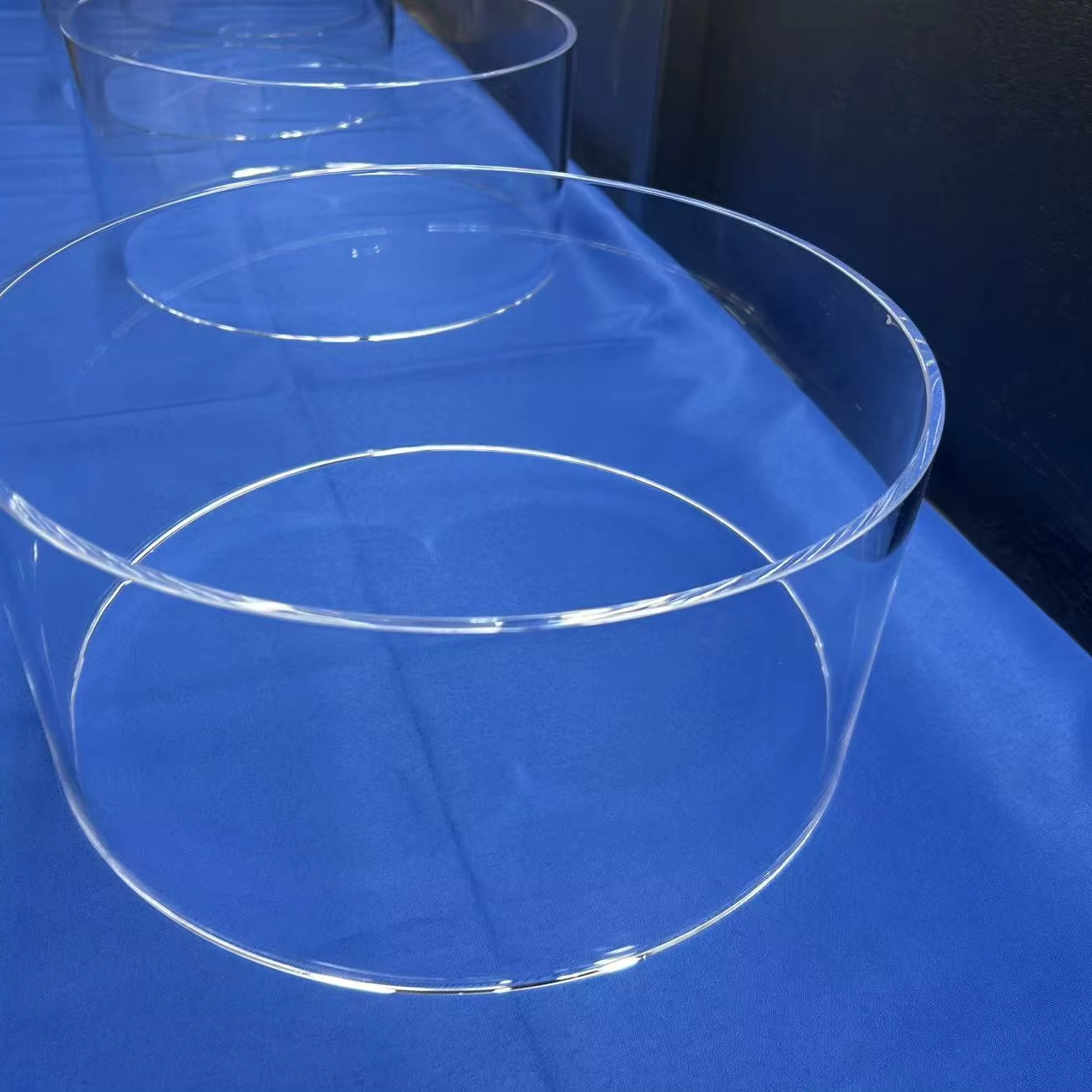
Large-Diameter Quartz Tubes Cutting & Welding
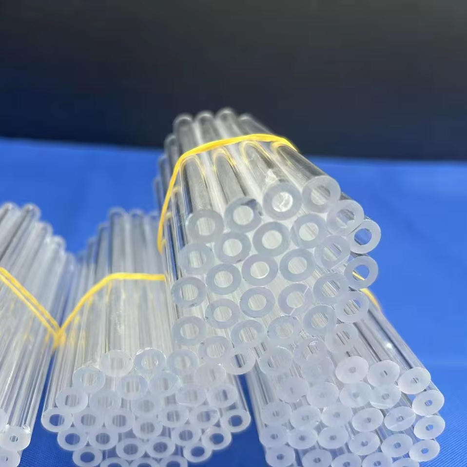
Customized Size Clear Quartz Test Tube
1. Precision Quartz Glass Rings: Material Science & Technical Capabilities
High-purity quartz glass rings represent a critical component category across sub-micron semiconductor fabrication, high-intensity plasma etching systems, optical instrumentation, and solar photovoltaic wafer manufacture. Operating under severe operational environments involving thermal shock up to 1450°C, corrosive gas attack (fluorine and chlorine chemistry), and intense UV or plasma radiation, precision quartz rings must maintain absolute dimensional stability, zero outgassing, and minimal trace metallic contamination.
Material Grade Selection Matrix (JGS1, JGS2, JGS3 & Synthetic Silica)
Selecting the optimal quartz grade is paramount to balancing optical performance, chemical purity, and material cost. Donghai County Nivra Quartz Products Co., Ltd. processes natural refined quartz and synthetic silicon tetrachloride precursors to yield four distinct optical and structural grades:
| Quartz Material Grade | SiO₂ Purity Level | OH- Content (PPM) | Spectral Transmission Range | Primary Industrial Application |
|---|---|---|---|---|
| JGS1 (Synthetic Fused Silica) | ≥ 99.999% (5N) | < 5 ppm to 1000 ppm | 185 nm – 2500 nm (Deep UV) | Semiconductor Photolithography, Laser Optics, UV Quartz Rings |
| JGS2 (Optical Grade Fused Quartz) | ≥ 99.99% (4N) | 150 ppm – 300 ppm | 220 nm – 2500 nm (UV-Visible) | View Ports, Chamber Sight Rings, Optical Substrates |
| JGS3 (Infrared Fused Quartz) | ≥ 99.99% (4N) | < 5 ppm (Low Hydroxyl) | 260 nm – 3500 nm (Near-IR / IR) | IR Spectroscopy Windows, Thermal Sensors, High-Temp Seals |
| Electric Arc / Opaque Quartz | ≥ 99.95% | Variable | Diffuse / Opaque | Furnace Insulation Rings, Heat Shield Collars, Solar Crucibles |
Technical Performance Metrics & Physical Properties
The operational longevity of a quartz ring within semiconductor etching chambers (such as reactive ion etching - RIE and inductively coupled plasma - ICP) directly correlates with material density and trace element concentration. Impurities such as Iron (Fe), Aluminum (Al), Sodium (Na), and Potassium (K) must be held strictly below critical parts-per-billion (ppb) thresholds to prevent wafer contamination during high-temperature thermal oxidation and diffusion processes.
2. Advanced Precision Manufacturing & Processing Technologies
To meet modern OEM specifications, manufacturing quartz rings extends far beyond basic glass blowing. It requires 5-axis CNC ultrasonic diamond milling, stress-free optical annealing, laser interferometry testing, and chemical surface passivation.
CNC Machining & Drilling
Utilizing high-speed CNC centers equipped with ultrasonic diamond tools, we execute inner/outer diameter grinding, beveling, counter-boring, and micro-hole drilling down to ±0.005mm tolerances without micro-chipping.
Flame & Optical Polishing
Depending on the required surface finish, we offer mechanical optical polishing achieving surface roughness Ra < 0.2 nm for optical transmission, or hydrogen-oxygen flame glazing for pristine edge seal integrity.
Stress Relief Annealing
Thermal stress generated during hot-working or heavy machining is eliminated using computer-controlled electric annealing kilns, holding ramps at 1150°C to guarantee zero internal birefringence or deformation under heat.
Erosion Resistance in Plasma Processing Environments
In modern semiconductor dry etching (fluorine-based chemistries such as CF4, SF6, and NF3), standard glass rings degrade rapidly due to chemical ion bombardment. High-purity synthetic fused quartz rings exhibit lower etch rates, minimizing particulate generation and extending process kit replacement intervals in 200mm and 300mm wafer fabrication lines.
3. Strategic Procurement Trends: 2025–2030 Outlook
As global supply chains adjust to advanced semiconductor manufacturing nodes (sub-3nm lithography), photovoltaic cell efficiency targets (TOPCon and Perovskite-Silicon tandems), and ultra-precise optical sensors, B2B quartz procurement priorities are undergoing structural shifts.
1. Dominance of Synthetic Quartz in Plasma Etching Chambers
While natural clear fused quartz remains cost-effective for standard furnace tubes and sight glasses, leading semiconductor fab buyers are increasingly standardizing on synthetic fused silica (JGS1 class) for focus rings and gas distribution rings. Synthetic quartz offers near-zero bubble content (Class 0 according to ISO standards) and total trace metal levels under 0.1 ppm, substantially extending ring life under aggressive halogen plasma exposure.
2. Demand for Large-Diameter & Ultra-Thin Geometry Capabilities
The expansion of 300mm wafer fabrication facilities worldwide has increased the demand for large-diameter quartz rings (outer diameters exceeding 450mm to 650mm) while maintaining exceptionally tight flatnesses (< 0.02mm) and parallelisms. Suppliers with integrated large-scale CNC machining and precision grinding tables hold a distinct competitive edge.
3. Circular Economy & Quartz Component Remanufacturing
Rising raw material costs and sustainability mandates are driving semiconductor manufacturers to adopt structured refurbishment programs. Used quartz focus rings and process flanges undergo chemical cleaning, fire-polishing, re-machining, and stress annealing to restore original OEM specifications at 40-60% of the cost of new components.
4. Rigorous Traceability & Digital Quality Records
Global procurement teams now require complete batch traceability, including Glow Discharge Mass Spectrometry (GDMS) material certification, 3D Coordinate Measuring Machine (CMM) dimensional reports, and spectroscopic transmission curves delivered electronically prior to shipment dispatch.
4. Donghai Nivra Quartz: Enterprise Advantages & OEM/ODM Excellence
Based in Donghai County, Lianyungang, Jiangsu — world-renowned as China's premier raw crystal and high-purity quartz cluster — Donghai County Nivra Quartz Products Co., Ltd. operates as a specialized manufacturer and exporter serving global industrial and research clients.
Situated directly at the heart of China’s largest quartz refining hub, we secure direct access to high-purity silica sand and high-purity optical raw ingots, ensuring cost efficiency and robust raw material inventory stability.
Our 101–200 skilled workforce operates advanced glass lathes, CNC machining centers, slotting tools, surface grinders, and fire-polishing stations. By keeping 100% of processing in-house, we control tolerance, clarity, and turn-around times.
Every quartz ring, sheet, and tube undergoes dimensional verification with digital micrometers and CMM equipment, surface defect inspection under high-intensity illumination, and stress pattern checking with polariscopes.
Fragile quartz rings are individually washed, vacuum sealed in cleanroom bags, and encased in custom-cut shock-absorbing EPE foam within sturdy export wooden crates, ensuring zero transit damage across air, sea, or express routes.
5. Frequently Asked Questions (FAQ) for Quartz Sourcing
Addresses critical technical and commercial considerations for engineering buyers and procurement officers.
What dimensional tolerances can Nivra Quartz achieve for custom quartz rings?
Our standard CNC grinding tolerance for outer/inner diameters and thickness is ±0.05mm. For high-precision semiconductor etch rings or optical window seats, our fine-lapping and diamond grinding processes can achieve outer diameter tolerances of ±0.005mm, flatness under 0.01mm, and parallelism under 0.008mm according to customer technical drawings.
How do I choose between JGS1, JGS2, and JGS3 quartz material for my application?
Choose JGS1 (synthetic silica) if your application involves deep-UV transmission (185–250nm), excimer laser optics, or ultra-clean semiconductor plasma etch chambers requiring <0.1 ppm trace metals. Select JGS2 for general optical windows, sight glasses, and UV lamp covers operating in the 220–2500nm range. Opt for JGS3 for infrared applications up to 3500nm or thermal processes where low hydroxyl (OH < 5 ppm) content is mandatory to prevent thermal absorption bands.
What is the continuous operating temperature limit for clear fused quartz rings?
Clear fused quartz components can operate continuously at temperatures up to 1100°C (2012°F) and withstand short-term peak exposures up to 1450°C. The softening point is approximately 1683°C. If your process involves thermal cycling above 1150°C, please consult our engineering team to ensure proper wall thickness and stress relief annealing protocols.
What is your Minimum Order Quantity (MOQ) and sample lead time?
We accommodate both prototyping and high-volume production. For custom OEM quartz rings and specialized labware, the MOQ typically starts at just 1 to 10 pieces depending on geometry. Prototype sample fabrication generally takes 5 to 7 business days following technical drawing confirmation.
How do you ensure zero contamination for semiconductor-grade quartz components?
Post-machining, all semiconductor-grade quartz parts undergo ultrasonic acid etching (using diluted HF/HNO3 baths) to remove surface micro-cracks and metallic machining residues. Parts are rinsed in 18MΩ ultra-pure deionized water, dried under HEPA airflow, and double-bagged inside a Class 1000 cleanroom environment before shipment.
Can you manufacture quartz rings directly from CAD files (STEP / DWG)?
Yes. Our engineering department works natively with STEP, IGES, DWG, DXF, and PDF formats. We review 3D CAD models for manufacturability, wall thickness integrity, and stress points, providing detailed engineering feedback and quotes within 5 hours.
Request a Technical Quote for Custom Quartz Rings
Send us your drawings, CAD files, or required dimensions. Our engineering specialists will review material grades, machining feasibility, and respond within 5 hours with a factory-direct proposal.