Precision Optical Quartz Components & Engineered Substrates
Manufactured to sub-nanometer surface roughness, laser-grade wavefront accuracy, and tight dimensional tolerances for demanding semiconductor, spectroscopy, and industrial laser environments.
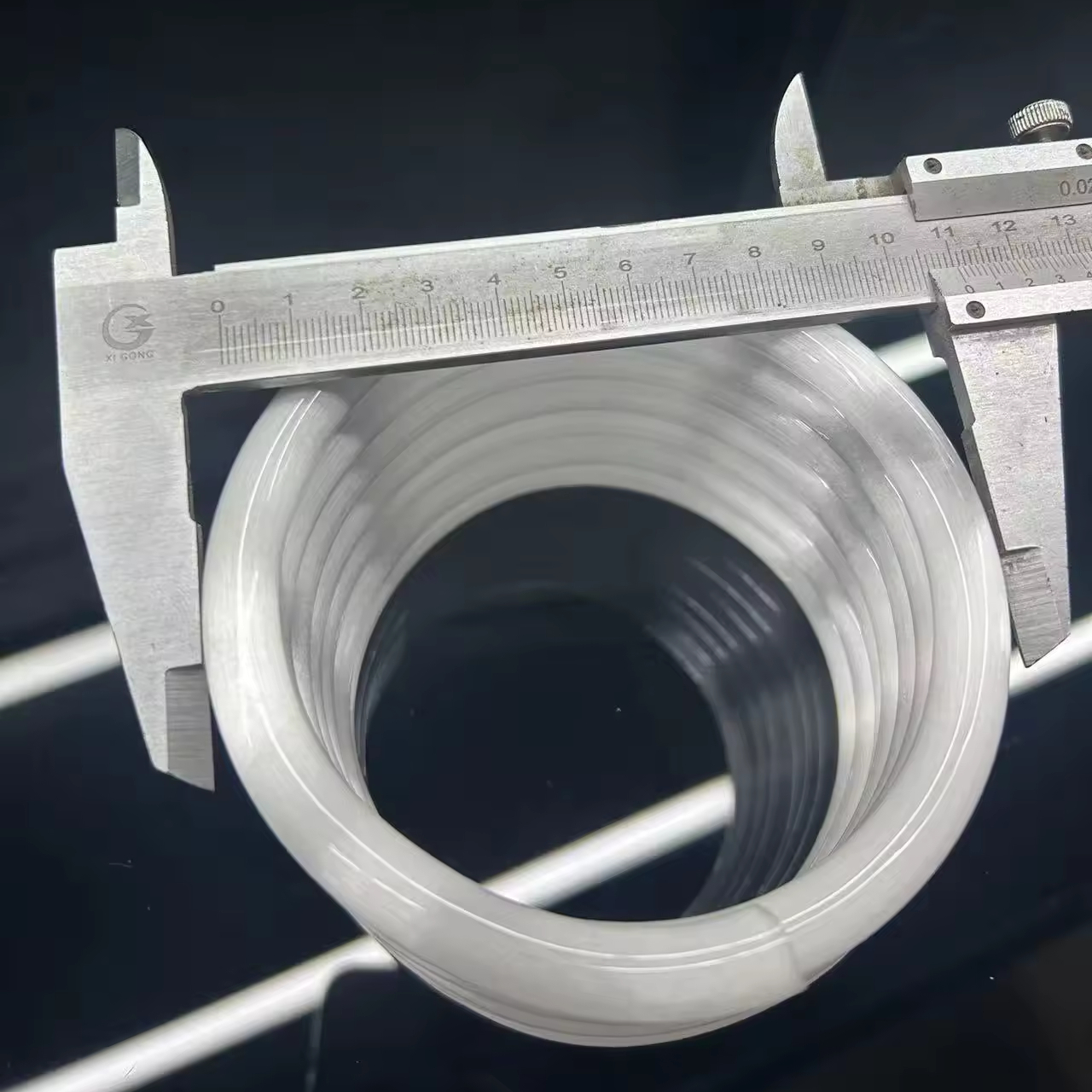
Helical Clear Quartz Glass Coil t Tube
High-transmission fused quartz helical heat exchange coil. Engineered for rapid fluid heating, vacuum plasma cooling, and high chemical resistance.
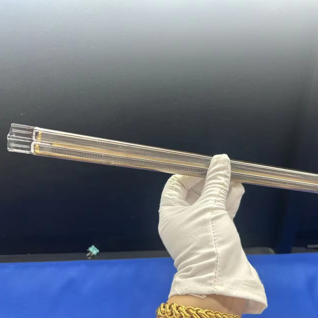
Graphene Quartz Heating Tube
Composite graphene electrothermal quartz radiator. Delivers instant infrared thermal radiation with 98.5% electro-thermal conversion efficiency.
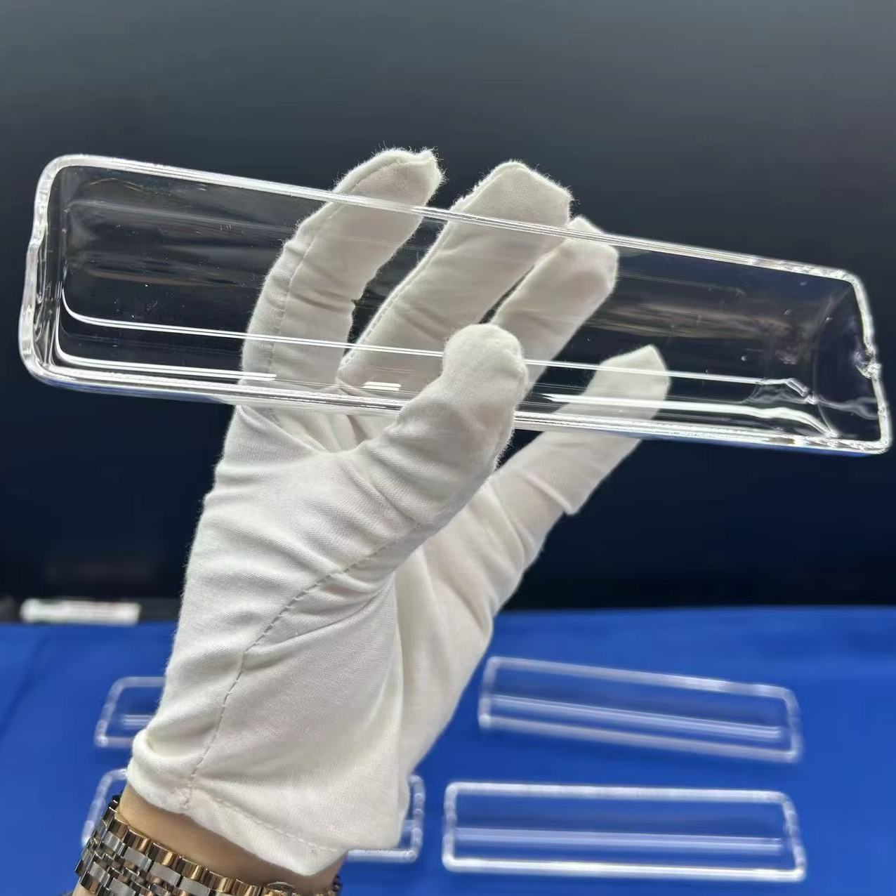
Customized Clear Fused Silica Quartz Boat Polished Clear Quartz Wafer Carrier
Ultra-pure fused silica slotted boat for 4/6/8/12-inch silicon wafer diffusion, LPCVD, and oxidation processes at continuous temperatures up to 1150°C.
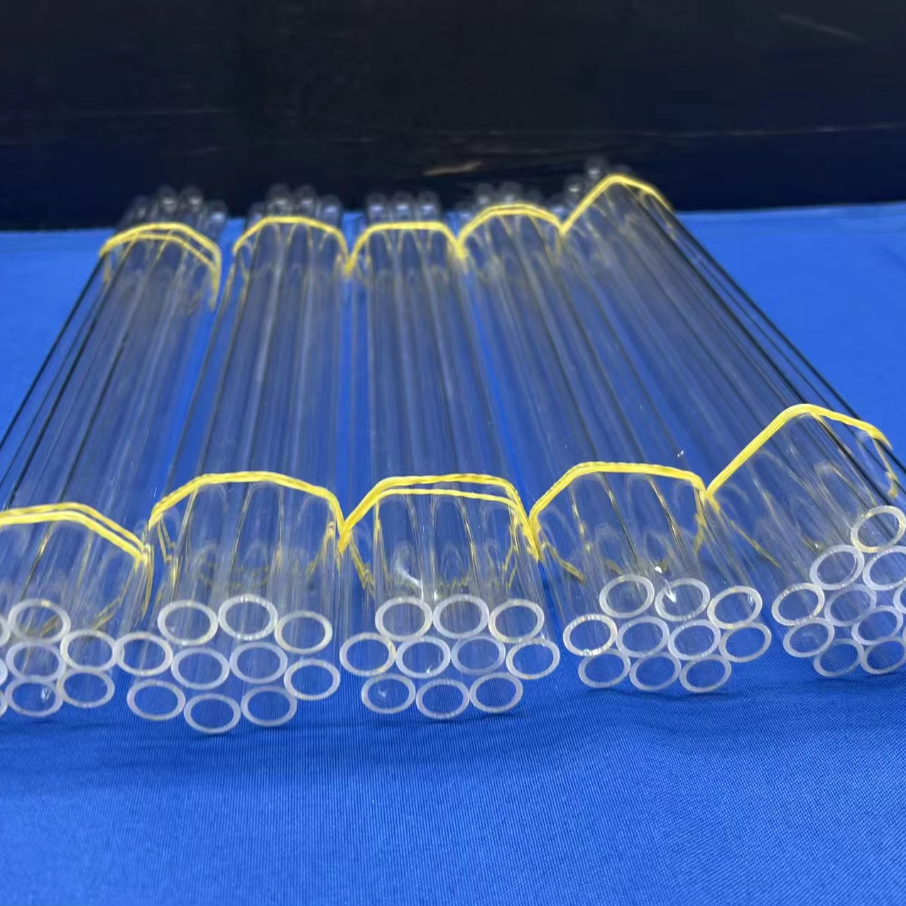
Quartz Test Tube
Optical-clarity analytical test tube featuring heavy-duty fire-polished rims, superior UV transmission, and zero thermal shock breakage during rapid flash cooling.
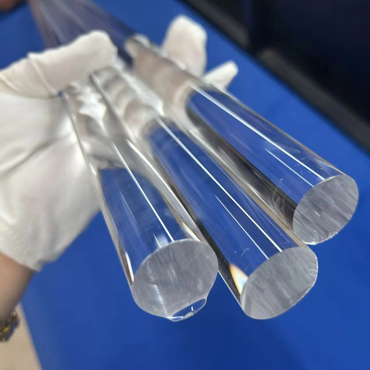
High-Purity Fused Quartz Large Diameter Round Rods (Cutting & Bending)
Large-diameter synthetic fused silica rods with comprehensive CNC slicing, fire-polishing, core drilling, precision grinding, and optical cylinder finishing.
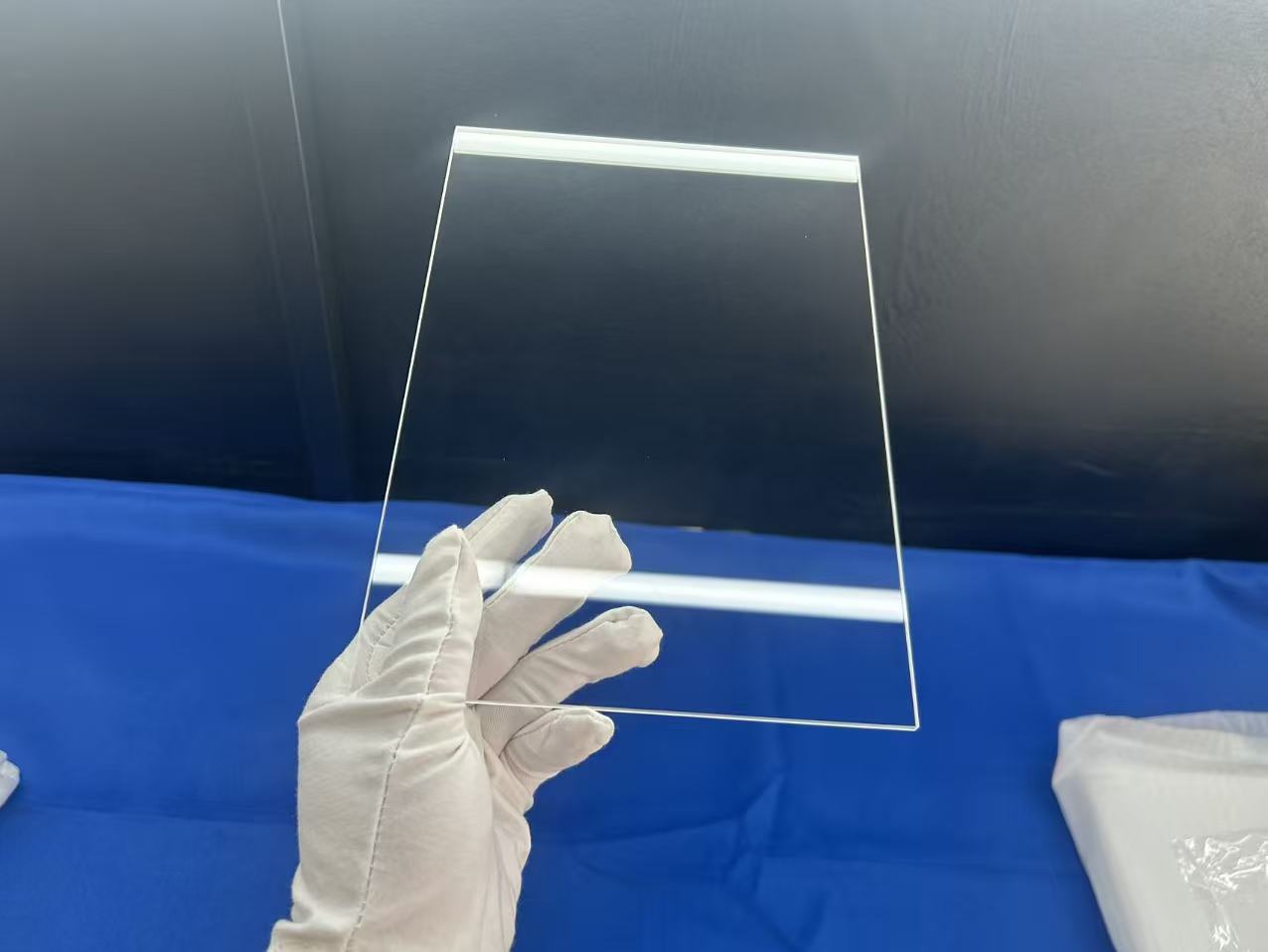
Custom Polished Transparent Square Quartz Glass Plate (3mm Laser Grade)
Double-side polished JGS1/JGS2 protective windows for multi-kilowatt fiber laser cutting heads. Scratch-dig 20/10, λ/4 optical flatness, and high damage threshold.
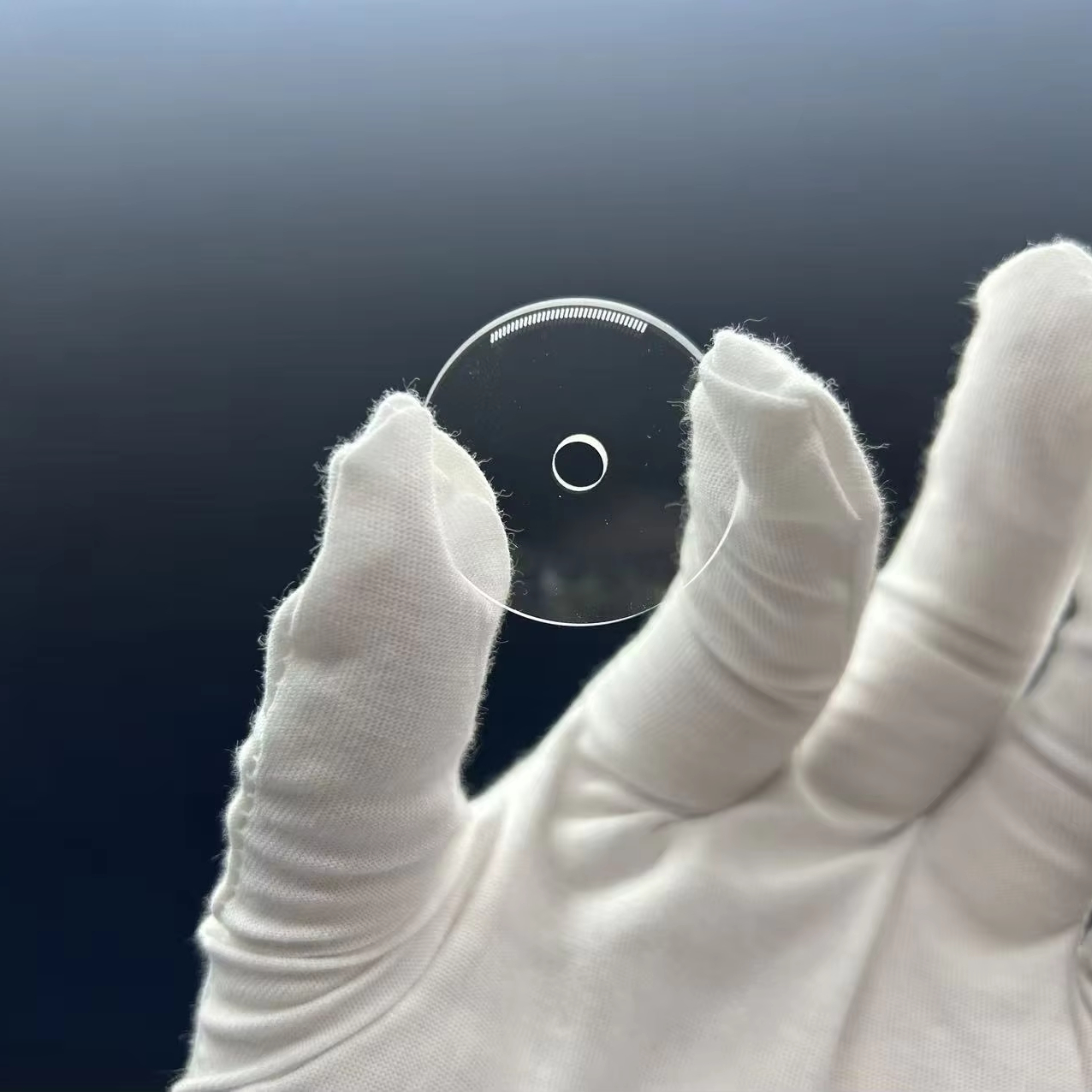
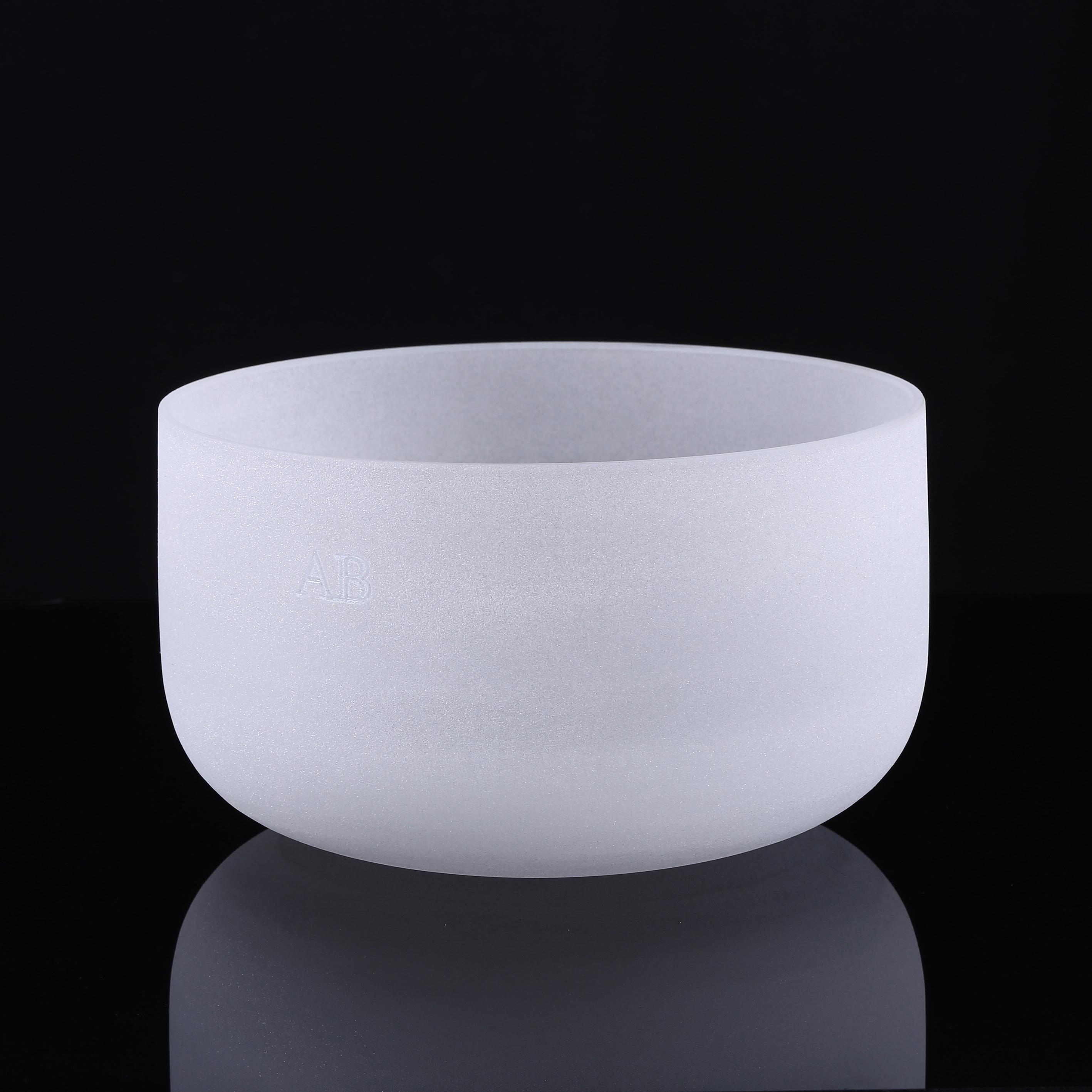
Frosted Quartz Sheet
Sandblasted and acid-etched light homogenizing quartz diffuser plate. Delivers isotropic beam scattering, uniform heat shielding, and chemical passivation.
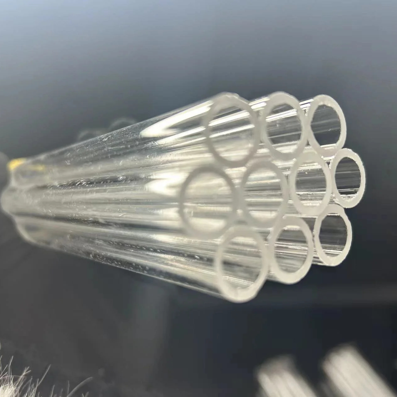
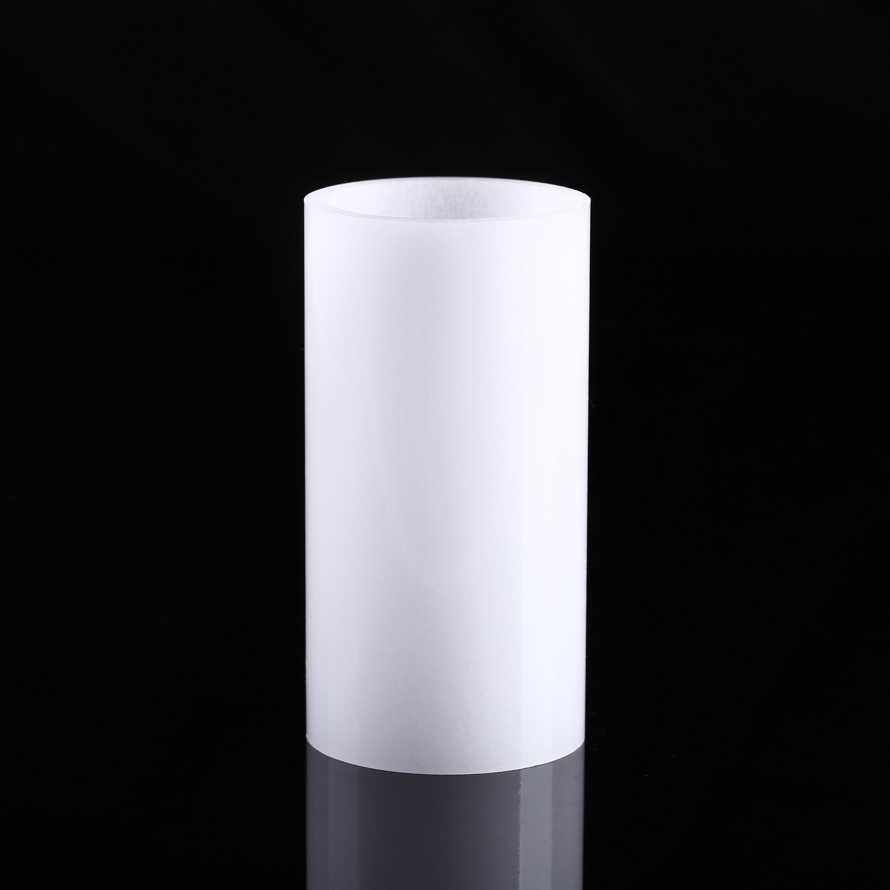
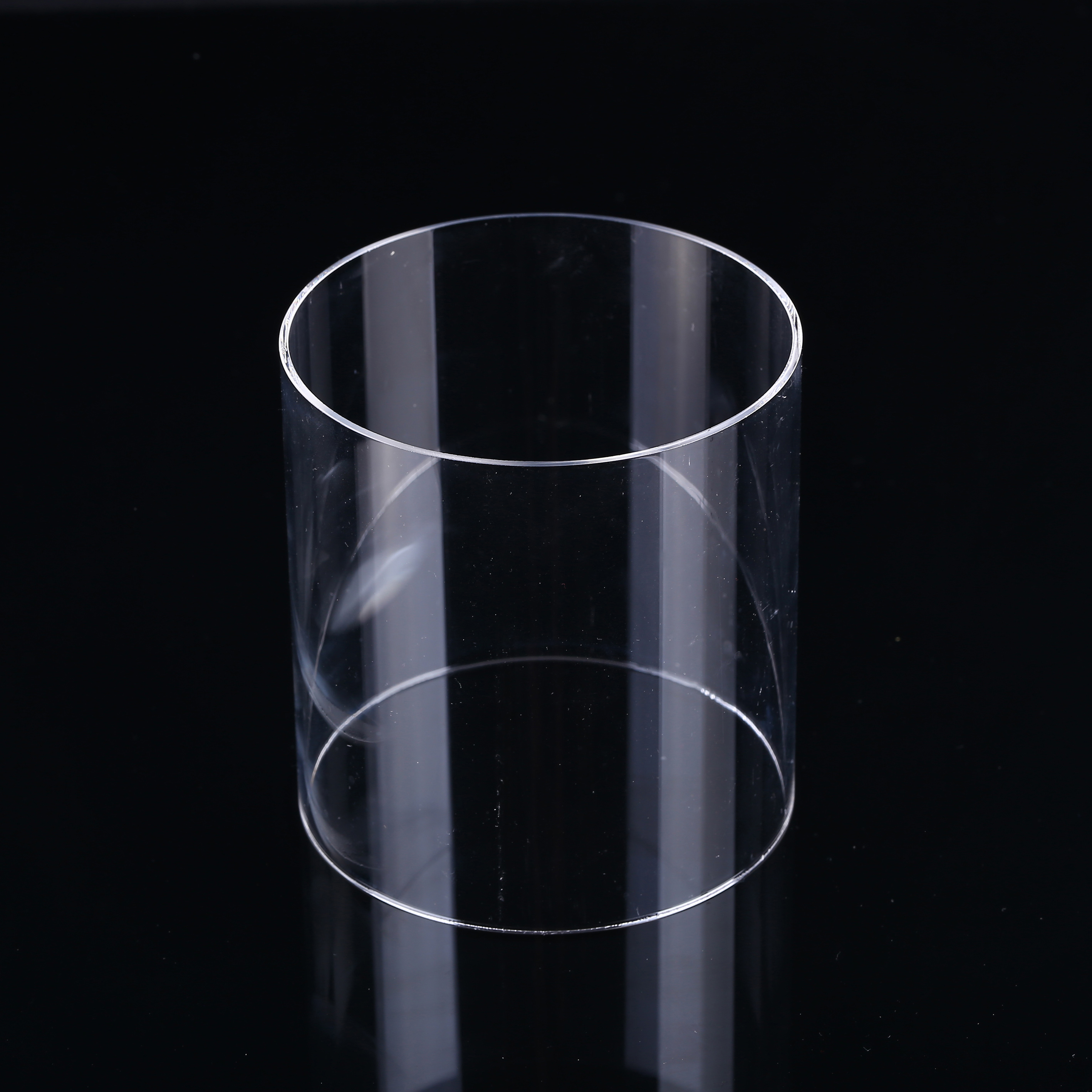
High-Temperature Transparent Quartz Cylinder Tube
Heavy-wall fused silica furnace process tubes. Extruded with minimal hydroxyl radical concentration, zero ovality variance, and thermal stability up to 1450°C.
Material Science of Optical Quartz: JGS1 vs. JGS2 vs. JGS3
Understanding the critical optical dispersion, hydroxyl ion (OH⁻) concentrations, and laser-induced damage thresholds (LIDT) across industrial fused silica variants.
Selecting the optimal optical quartz window substrate for precision scientific instrumentation, aerospace viewports, or semiconductor photolithography requires an exhaustive analysis of transmission spectra, material synthesis routes, and residual impurity matrices. While colloquial industry terminology often uses "fused quartz" and "fused silica" interchangeably, the mechanical, optical, and thermal behaviors of these polymorphs of silicon dioxide (SiO₂) diverge significantly based on their raw material origins and melting dynamics.
Natural Fused Quartz (Electrically or Flame Fused): Manufactured by fusing ultra-pure natural crystalline quartz sand (sourced from world-renowned deposits such as Donghai County, China, or Spruce Pine, North Carolina). This material offers superior structural viscosity at elevated temperatures, excellent mechanical hardness, and high thermal stability up to 1450°C. However, minor metallic trace elements (such as Aluminum at 15–30 ppm, Titanium at 1–2 ppm, and Iron at <0.5 ppm) introduce microscopic absorption bands in the deep ultraviolet range, making natural quartz best suited for visible, near-infrared, and thermal furnace applications (Grade JGS2).
Synthetic Fused Silica (CVD / VAD Gas Phase Synthesis): Produced through chemical vapor deposition using silicon tetrachloride (SiCl₄) or organic silanes reacting with oxygen in a high-temperature hydrogen flame. This chemical synthesis yields amorphous silica with total metallic impurity levels below 0.1 ppm (99.9999% purity). Free from micro-inclusions, striae, and crystalline seed defects, synthetic fused silica (Grade JGS1) guarantees near-theoretical optical transmission down to 185 nm in the deep ultraviolet (DUV), completely eliminating optical solarization and bubble-induced laser scatter.
| Optical Grade | Material Type | Spectral Transmission | OH⁻ Content | Typical LIDT (@ 1064nm, 10ns) | Primary Applications |
|---|---|---|---|---|---|
| JGS1 | Synthetic Fused Silica | 185 nm – 2500 nm | ≤ 1200 ppm | > 15 J/cm² | Excimer lasers, DUV lithography, UV spectrometer windows, fluorescence analysis |
| JGS2 | Optical Fused Quartz | 220 nm – 2500 nm | ≤ 200 ppm | > 8 J/cm² | Industrial sight glasses, UV-Vis spectrophotometers, furnace observation ports |
| JGS3 | Low-OH Infrared Quartz | 260 nm – 3500 nm | ≤ 5 ppm | > 12 J/cm² | IR pyrometry windows, Nd:YAG / Fiber laser optics, CO₂ laser monitoring |
| Corning 7980 Eq. | Ultra-High Purity Silica | 190 nm – 2100 nm | 800 – 1000 ppm | > 18 J/cm² | Semiconductor stepper projection lenses, high-energy laser beam splitters |
| Sapphire (Al₂O₃) | Single Crystal Sapphire | 200 nm – 5000 nm | Non-hydrated | > 10 J/cm² | Extreme pressure viewports, scratch-resistant defense windows, sensor covers |
Thermomechanical & Physical Benchmark Values
Fused quartz exhibits an extraordinarily low coefficient of thermal expansion (CTE ≈ 5.5 × 10⁻⁷ /°C from 20°C to 320°C), roughly 1/30th that of standard soda-lime float glass and 1/6th that of borosilicate 3.3. This near-zero thermal expansion endows quartz windows with unmatched thermal shock resistance; an optical flat can be heated to 1100°C in a muffle furnace and plunged directly into ice water without micro-fracturing or dimensional warping.
| Physical / Mechanical Property | Experimental Test Value | Standard Testing Reference | Engineering Advantage |
|---|---|---|---|
| Refractive Index ($n_d$ @ 587.6 nm) | 1.4585 | Abbe Refractometry | Low optical dispersion (Abbe Number $V_d = 67.8$), minimizing chromatic aberrations. |
| Density (ρ) | 2.20 ± 0.01 g/cm³ | Archimedes Immersion | Lightweight structural integrity for aerospace payload optics and aerial pods. |
| Knoop Hardness (HK) | 520 – 600 kgf/mm² (Mohs 5.5–6.5) | ASTM E384 | Superior scratch resistance against harsh abrasives, sandstorms, and slurry impingement. |
| Young’s Modulus ($E$) | 72 – 74 GPa | Ultrasonic Pulse Echo | High structural rigidity, resisting vacuum deformation under high differential pressures. |
| Thermal Shock Gradient (ΔT) | > 1000 °C Differential | Water Quenching Cycle | Immune to laser thermal runaway and extreme cryogenic-to-furnace temperature swings. |
| Softening Point | 1683 °C ± 20 °C | Dilatometric Extrusion | Continuous high-temperature operation up to 1100 °C; short-term survival to 1450 °C. |
Future Procurement Trends in Precision Optical Quartz (2025–2030)
How advancing lithography, ultra-high-power fiber lasers, and agile supply chain architectures are reshaping optical component specifications worldwide.
1. Laser Power Escalation to 30kW–60kW
With fiber lasers expanding from 12kW to 30kW+ for shipyard cutting and EV battery manufacturing, optical window procurement is shifting from standard JGS2 to low-absorption synthetic silica with Ion-Beam Sputtered (IBS) coatings to prevent thermal lensing and focal point drift.
2. Demand for Sub-Angstrom Super-Polishing
Semiconductor metrology and quantum photonics require optical quartz flats with surface roughness $R_a < 0.2\text{ nm}$ (sub-angstrom level). Procurement contracts increasingly mandate white-light interferometry and Zygo Verifire 3D maps to eliminate stray light scattering.
3. Direct-to-Source Supply Consolidation
Western optical engineering conglomerates are bypassing intermediaries and contracting directly with manufacturing clusters in Donghai, Jiangsu. This direct OEM engagement lowers bill-of-materials costs by 30%–45% while slashing custom prototype iteration times from 12 weeks to 14 days.
4. Strict Cleanliness & ISO 14644 Compliance
Procurement terms now enforce ISO Class 5 / Class 6 cleanroom double-vacuum packaging. Optical quartz windows destined for vacuum chambers and semiconductor process lines must arrive particle-free, hydrocarbon-degreased, and sealed in antistatic nitrogen blister packs.
5. Complex Geometry & Metalized Hermetic Sealing
Standard round and square viewports are being superseded by monolithic step-profile windows, CNC-profiled beveled prisms, and solderable metallized edges (Titanium-Platinum-Gold sputtering) designed for direct brazing onto ultra-high vacuum (UHV) stainless steel flanges.
6. Environmental Traceability & Low-Carbon Fusion
European and North American buyers increasingly require RoHS, REACH, and full conflict-mineral-free certifications, accompanied by supply chain verification showing energy-efficient electric-arc or oxygen-hydrogen combustion furnaces during primary ingot refining.
Donghai County Nivra Quartz Products Co., Ltd.
Founded in February 2019 in Donghai County, Lianyungang, Jiangsu — China’s world-renowned crystal and quartz capital. Operating as an audited manufacturer and exporter with 101–200 skilled personnel.
Donghai Epicenter Sourcing
Direct access to world-class silicon raw material deposits, significantly reducing feed-stock freight costs and guaranteeing consistent silica batch purity.
Precision Metrology Lab
Equipped with laser interferometers, UV-Vis-NIR dual-beam spectrophotometers, coordinate measuring machines (CMM), and optical goniometers.
Proven Export Track Record
Serving Tier-1 OEM accounts across North America (40%), Western Europe (20%), Eastern Europe (14%), and South America (11.4%) with a 5.0/5 customer satisfaction score.
Rapid Engineering Turnaround
Average inquiry response within 5 hours, engineering DFM feedback within 24 hours, and expedited 7-day delivery for urgent prototype wafer batches.
Operating strictly under audited ISO 9001 and CE compliance standards. On-site verified premises at 285 Heping East Road, Lianyungang, Jiangsu, China.
Send an InquiryOEM/ODM Precision Optical Machining Capabilities
Comprehensive manufacturing capabilities for custom optical flats, high-pressure vacuum viewports, round discs, step windows, and laser debris shields.
| Machining Parameter | Commercial Grade Specification | High-Precision Optical Grade | Laser / Semiconductor Ultra-Grade |
|---|---|---|---|
| Diameter / Dimension Range | Ø 2.0 mm – 1500 mm | Ø 5.0 mm – 800 mm | Ø 10.0 mm – 450 mm |
| Dimensional Tolerance | ± 0.10 mm (± 0.004") | ± 0.025 mm (± 0.001") | ± 0.005 mm (± 0.0002") |
| Thickness Tolerance | ± 0.10 mm | ± 0.02 mm | ± 0.005 mm |
| Surface Figure (Transmitted Wavefront) | 1 λ – 2 λ per 25 mm @ 632.8 nm | λ / 4 – λ / 8 per 25 mm | ≤ λ / 10 – λ / 20 Total Transmitted Flatness |
| Surface Quality (MIL-PRF-13830B) | 80 / 50 Scratch-Dig | 40 / 20 Scratch-Dig | 10 / 5 – 0 / 0 (Laser Cavity Grade) |
| Surface Roughness ($R_a$) | < 1.5 nm RMS | < 0.5 nm RMS | ≤ 0.15 nm RMS (Super-Polished) |
| Parallelism / Wedge Angle | < 3 arc minutes | < 30 arc seconds | ≤ 5 – 10 arc seconds (< 0.025 mm wedge) |
| Edge Treatment & Bevel | Standard commercial cut | 0.2 – 0.5 mm × 45° protective chamfer | Ground & fire-polished CNC precision bevel, zero micro-chipping |
| Anti-Reflective Thin-Film Coatings | Uncoated / Commercial AR ($R < 1.5\%$) | Single-Layer MgF₂ / BBAR ($R < 0.5\%$) | IAD / IBS V-Coating ($R < 0.1\%$ @ specified laser line) |
Structural Window Thickness Sizing for Vacuum & High-Pressure Vessels
A common engineering failure mode in vacuum chamber design is selecting an optical window that is too thin, resulting in mechanical rupture under atmospheric pressure differential, or choosing an excessively thick substrate that induces optical aberrations and unnecessary thermal mass. To ensure operator safety and compliance with ASME Pressure Vessel codes, window thickness $t$ must be calculated using the clamped circular plate formulation:
$$t = \sqrt{\frac{1.063 \cdot D^2 \cdot \Delta P \cdot SF}{4 \cdot M_R}}$$ Where: $D$ = Unsupported clear aperture diameter (mm); $\Delta P$ = Differential pressure applied across the window (MPa); $SF$ = Engineering safety factor (minimum 4 for non-critical, recommended 8–10 for toxic/flammable gas or personnel safety); $M_R$ = Modulus of Rupture of fused silica ($M_R \approx 48 \text{ to } 52\text{ MPa}$ at 20°C).
Our technical application engineers in Donghai perform finite element analysis (FEA) and stress birefringence inspections on all custom pressure window orders to verify that mounting gasket torque does not introduce localized mechanical stress concentrations, which could cause catastrophic optical failure under thermal cycling.
Frequently Asked Questions About Optical Quartz Window Sourcing
Direct technical answers to common queries regarding material selection, optical damage thresholds, custom drawings, and global logistics.
How do I choose between JGS1, JGS2, and JGS3 for my application?
Selection is dictated by your system's operational optical spectrum and acceptable thermal absorption. If your system operates in the deep ultraviolet (185 nm – 300 nm), such as excimer laser optics, semiconductor photolithography, or UV sterilization monitoring, JGS1 Synthetic Fused Silica is required to ensure 90%+ UV transmission and prevent solarization. If your application is in the visible to near-infrared spectrum (380 nm – 2000 nm), such as industrial sight glasses, boiler viewports, or low-cost laser covers, JGS2 Fused Quartz offers excellent cost efficiency. For applications operating between 2000 nm and 3500 nm (infrared sensors, thermal pyrometers, or high-power 1064/2100nm lasers), JGS3 Low-OH Fused Quartz is necessary to eliminate the severe hydroxyl (OH⁻) absorption dip at 2730 nm.
What Laser-Induced Damage Threshold (LIDT) can Nivra Quartz windows achieve?
Uncoated laser-grade JGS1 synthetic fused silica substrates manufactured in our facility achieve an LIDT exceeding 15 to 20 J/cm² @ 1064 nm, 10 ns pulse width, 20 Hz repetition rate. When finished with our Ion-Assisted Deposition (IAD) dielectric anti-reflective V-coatings, the composite optics achieve certified ratings of > 10 J/cm² at 1064 nm and > 5 J/cm² at 532 nm / 355 nm. Every high-power laser optics batch includes spectrometer transmission traces and raw ingot batch trace reports upon request.
Can you fabricate custom optical quartz windows from our 2D/3D engineering drawings?
Yes. As an OEM/ODM specialist, over 70% of our output is custom-machined. We accept engineering CAD files in PDF, DXF, DWG, STEP, IGES, and SolidWorks formats. Our multi-axis CNC machines, ultrasonic drillers, and double-sided planetary polishers can produce complex non-circular geometries, step windows, counter-bored holes, internal bevels, laser markings, and prism wedges down to ±0.005 mm mechanical precision.
What is your Minimum Order Quantity (MOQ) and sample lead time?
We maintain a flexible manufacturing policy to support both R&D engineering prototyping and multi-thousand piece volume manufacturing. For standard dimensional discs and rectangular blanks, the MOQ is 1 to 10 pieces. For complex custom-tooled configurations, prototyping batches typically start at 5 to 20 pieces. Standard sample lead time is 7 to 10 business days, with expedited 48-hour turnarounds available for urgent wafer development programs.
How do you ensure fragile precision optical components arrive intact overseas?
Our export packaging engineered for international air and ocean freight eliminates transit damage. Precision polished optics are individually inspected, cleaned with electronic-grade solvents, and sealed inside antistatic PET blister boxes or lens tissue wraps. Components are cushioned within custom-molded high-density polyethylene (EPE) shock-absorbing foam inserts and encased in heavy-duty 5-ply export cartons or fumigation-free solid plywood crates. Our international breakage rate remains below 0.05% across thousands of shipments.
What optical metrology and quality inspection reports are provided with orders?
Every production batch leaves our Donghai facility accompanied by a comprehensive Certificate of Conformance (CoC). Depending on your PO specification requirements, we provide: (1) Zygo 3D surface flatness interferograms (λ/10 data), (2) PerkinElmer UV-Vis-NIR spectral transmission curves, (3) Optical micrometer dimensional measurement reports, and (4) Raw material melt chemistry certificates confirming 99.99%+ SiO₂ purity and OH⁻ ppm levels.
How does quartz compare against sapphire and borosilicate glass for sight windows?
Compared to Borosilicate Glass, fused quartz provides a continuous operating temperature 650°C higher (1100°C vs 450°C), superior UV transmission (>90% at 200nm vs 0% for borosilicate), and six times lower thermal expansion, completely eliminating thermal shock fracture. Compared to Single Crystal Sapphire, fused quartz is roughly 40% to 60% more cost-effective, can be produced in much larger aperture diameters (up to 1500 mm vs ~300 mm practical limit for sapphire), and does not exhibit optical birefringence, which can distort polarized laser beams.
Request a Fast Engineering Review & Quotation
Send us your target dimensions, required optical quartz grade (JGS1 / JGS2 / JGS3 / Sapphire), surface scratch-dig tolerances, and estimated batch volume. Our technical engineering team in Donghai will analyze your drawing and respond with DFM feedback within 5 hours.
Send an Inquiry