OEM Fused Quartz Components & Specialized Substrates
Direct from our manufacturing facility in Donghai County: standard inventory and full custom dimensioning according to customer CAD, DWG, and STEP specifications.
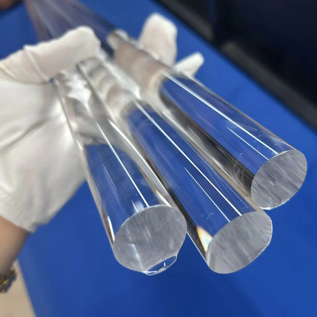
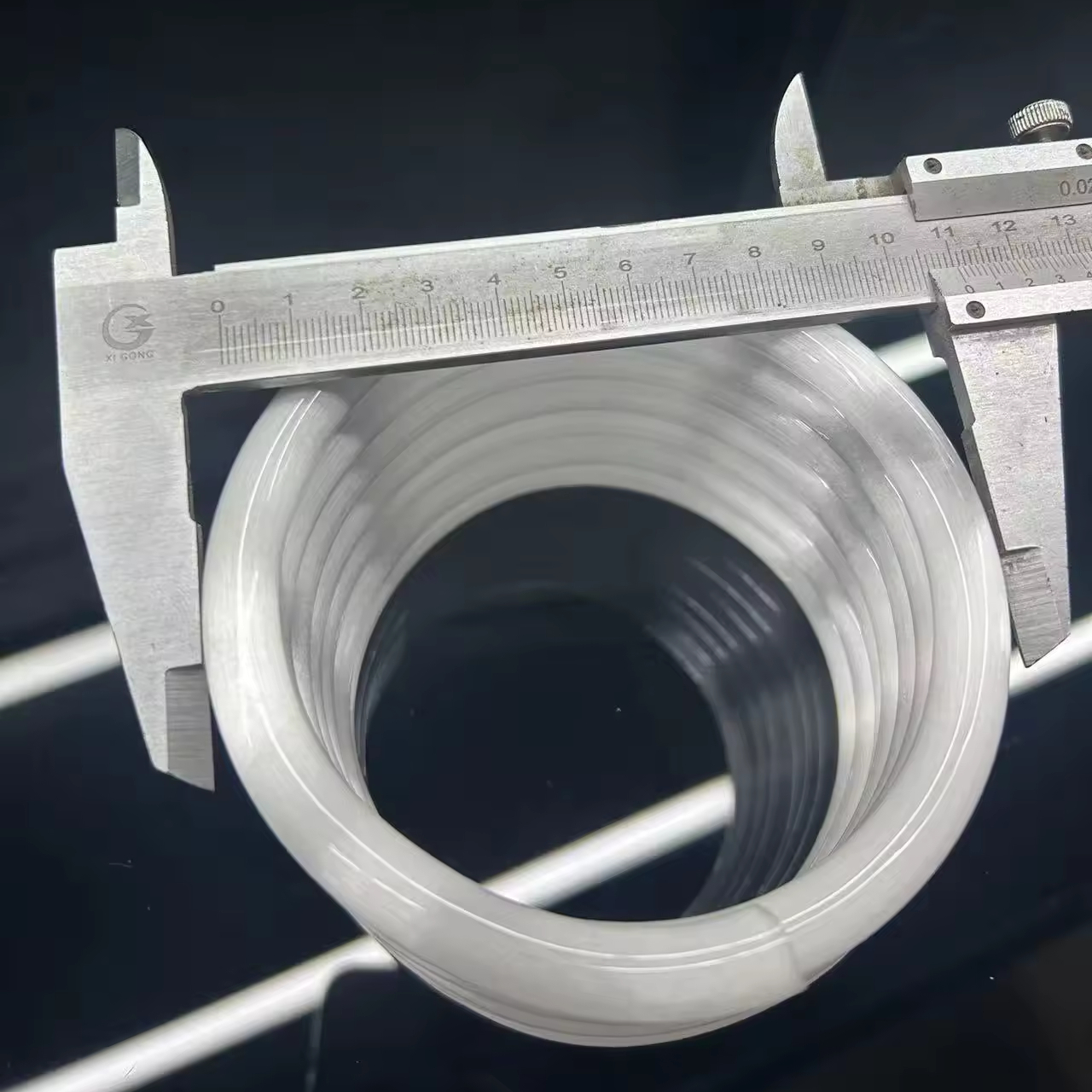
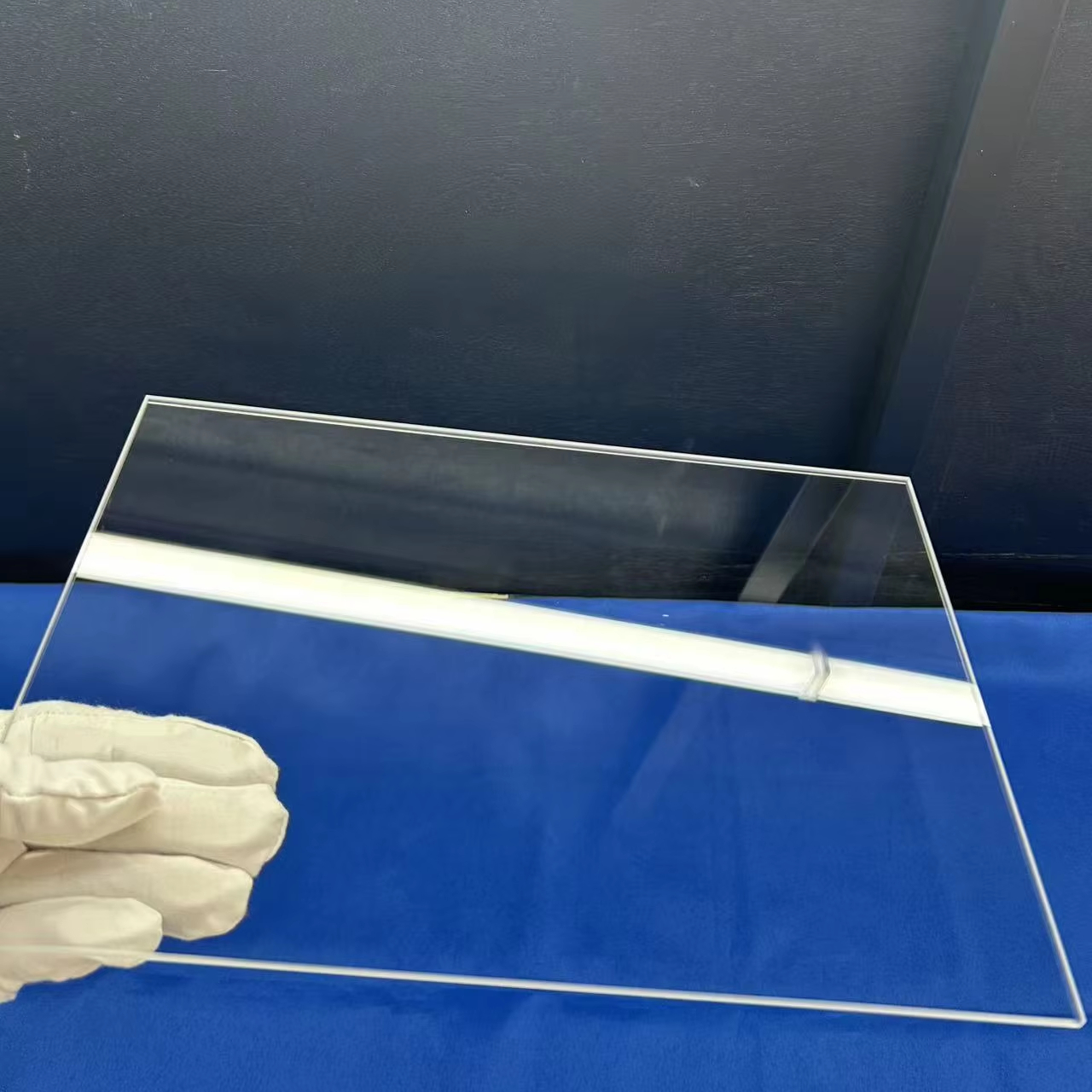
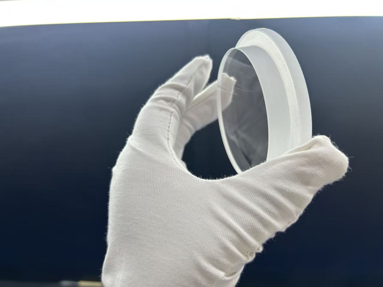
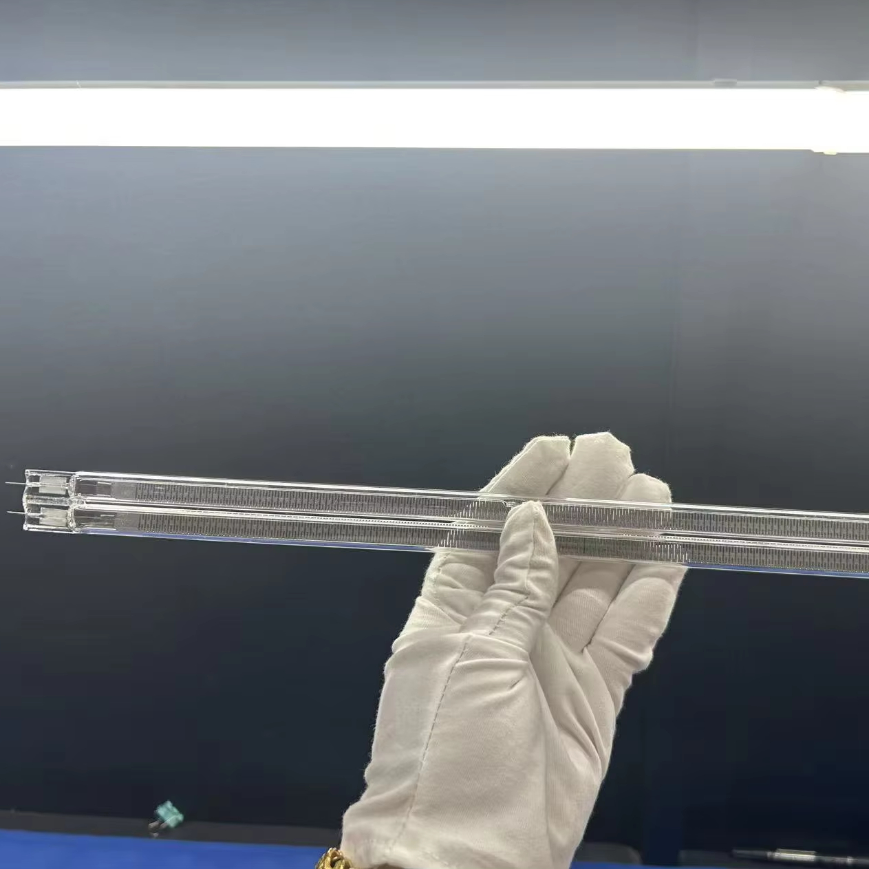
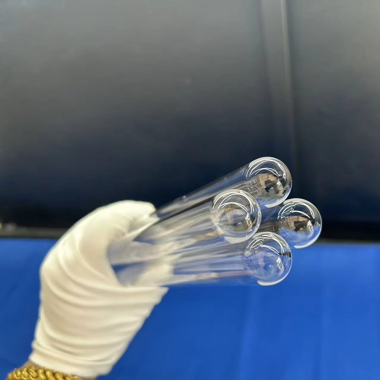
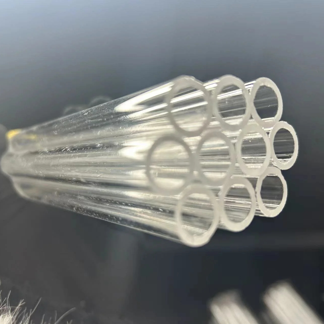
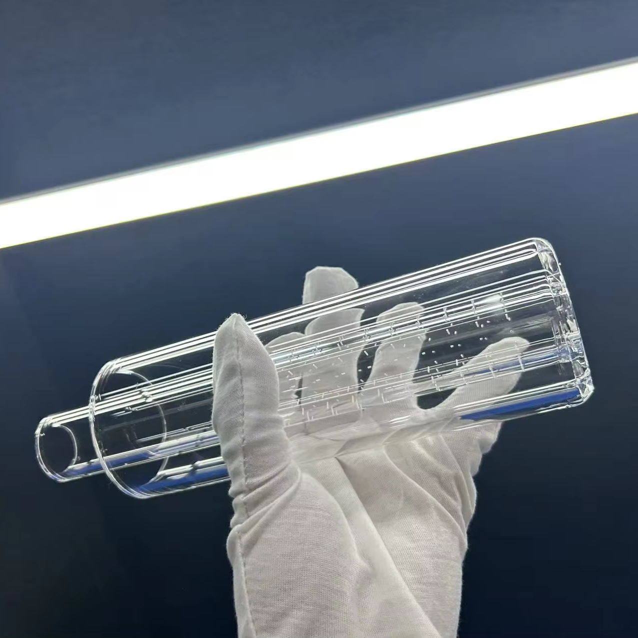
Material Science Foundations: Synthetic Fused Silica vs. Natural Fused Quartz Discs
When selecting a custom OEM fused quartz disc, industrial engineers must distinguish between natural electric-arc fused quartz and synthetic fused silica produced via chemical vapor deposition (CVD). Natural fused quartz, synthesized from beneficiated silica sand originating in geological deposits like Donghai County, offers supreme structural stiffness, exceptional thermal resilience (strain point at 1070°C, softening point at 1683°C), and low cost for thermal furnace sight windows and semiconductor diffusion boats.
Conversely, for UV photolithography, excimer laser windows, and precision interferometer flats, synthetic fused silica (such as JGS1, Corning 7980, or Suprasil equivalents) eliminates interstitial metallic impurities (Fe, Al, Ti, Na < 0.1 ppm). This results in unmatched UV spectral transmission reaching down to 185 nm without solarization or laser-induced micro-damage.
Key Optical & Physical Thresholds
- Thermal Expansion (CTE): 5.5 × 10⁻⁷ / °C (20°C to 320°C)
- Thermal Shock Parameter: Can withstand 1100°C quench into 20°C cold water
- Refractive Index (nd @ 587.6 nm): 1.4585 with low dispersion (Abbe νd = 67.8)
- Surface Roughness (Super-polished): Ra < 0.3 nm (3 Ångströms)
- Laser Damage Threshold (LDT): > 15 J/cm² @ 1064 nm (10 ns pulse)
| Quartz Grade | Spectral Range | OH Content | Bubbles / Inclusions (ISO 10110) | Primary Industrial Use-Case |
|---|---|---|---|---|
| JGS1 (Synthetic Silica) | 185 nm – 2500 nm (Deep UV) | ≈ 1200 ppm (High OH) | Class 0 (Bubble-free optical aperture) | EUV/DUV Optics, Laser Windows, Spectrophotometer Cuvettes |
| JGS2 (Optical Quartz) | 220 nm – 2500 nm (UV-Vis) | ≈ 150 – 200 ppm | Class 1 – 2 (Extreme micro-inclusion control) | High-temp Sight Glasses, Optical Discs, Wafer Inspection |
| JGS3 (Infrared Grade) | 260 nm – 3500 nm (IR / Full Vis) | < 5 ppm (“Water-free”) | Class 1 (Industrial Optical Standard) | FLIR Systems, IR Pyrometry Windows, Laser Cavities |
| Commercial Fused Quartz | 260 nm – 2800 nm | < 30 ppm | Class 2 – 3 (Homogeneous industrial grade) | Semiconductor Furnace Flanges, High-Power Lamp Jackets |
Emerging B2B Procurement Trends for Fused Quartz Discs
As global advanced manufacturing sectors scale toward sub-2nm nodes, megawatt lasers, and deep-space instrumentation, precision quartz procurement dynamics are fundamentally shifting.
1. Sub-Nanometer Surface Lapping & CMP Wafers
Global semiconductor fabrication plants are transitioning quartz carrier plates and witness discs from traditional mechanical polish to double-sided Chemical Mechanical Planarization (CMP). Sourcing directives now specify surface roughness below Ra 0.3 nm and total thickness variation (TTV) < 1.5 μm across 300 mm diameters to prevent focal distortion during advanced 3D packaging.
2. Supply Consolidation & Raw Material Provenance
With geopolitical raw material vulnerabilities impacting high-tech manufacturing, B2B procurement managers are actively bypassing multi-tier brokerages to contract directly with vertically integrated Chinese manufacturers situated in Donghai County. Controlling crystal purification, raw ingot melting, and secondary CNC edge grinding under one roof slashes lead times by 40% to 60%.
3. Ultra-High Power Laser & Extreme Environment Sight Glass Demands
As 20kW+ continuous-wave (CW) industrial fiber cutting lasers and fusion reactor inspection viewports proliferate, quartz discs require zero-stress annealing to eliminate localized internal birefringence (Δn ≤ 5 × 10⁻⁶). Buyers now demand batch-verified certification for wavefront flatness (λ/10 per 25mm) and strict scratch-dig inspection per MIL-PRF-13830B.
Why Tier-1 OEM Engineers Partner with Nivra Quartz
Headquartered at 285 Heping East Road, Lianyungang, Jiangsu — in China's silica and quartz capital — Donghai County Nivra Quartz Products Co., Ltd. bridges raw mineral excellence with certified nanoscale fabrication.
Epicenter Sourcing Economics
Situated in Donghai County, we tap directly into China's premier silica refining ecosystem. We offer raw material purity from 99.99% to 99.9999% SiO₂ at factory-direct pricing devoid of domestic dealer markups.
Full In-House Machining Suite
Our workshop houses high-precision CNC 5-axis routers, planetary double-sided lap-polishing machines, ultrasonic core drillers, laser slicing, and automated fire-polishing stations for turnkey geometry.
Metrology & Cleanroom QC
Every custom OEM fused quartz disc undergoes strict Zygo laser interferometer inspections for surface flatness, spectrophotometric transmittance verification, and Class 1,000 cleanroom vacuum packaging.
Global Safe-Transit Architecture
With 40% export share to North America and 30%+ to Western/Northern Europe, our specialized multi-tier vibration-damping cases and wooden crates ensure zero chipping or fracture during intercontinental transit.
Next-Gen Fabrication Capabilities
Selective Laser-Induced Etching (SLE): Creating 3D microfluidic internal channels inside monolithic quartz discs without adhesive interfaces.
Dielectric Thin-Film PVD Coatings: Dual-wavelength anti-reflective (AR) coatings offering reflectance R < 0.2% per surface at chosen laser wavelengths.
Ultra-Thin Precision Wafers: Polished quartz discs down to 50 μm thickness with total perimeter chamfering to prevent micro-fracture propagation.
Engineering Complex Geometries: From Stepped Sight Glasses to Micro-Hole Discs
Modern industrial applications no longer demand mere circular discs; they require highly integrated, functionalized sub-assemblies. Nivra Quartz leverages advanced multi-axis CNC profiling to fabricate counter-bored holes, beveled sealing perimeters, dual-layer stepped optical discs, and ultrasonic drilled arrays (down to 0.2 mm diameter perforations).
By coupling computerized dimensional grinding with thermal hydrogen-oxygen flame edge annealing, our finished quartz discs eliminate residual tensile stress concentrations, increasing mechanical burst strength under vacuum and hydraulic pressures by up to 35% compared to conventionally cut discs.
Frequently Asked Questions: Sourcing Custom OEM Fused Quartz Discs
Comprehensive engineering clarifications to assist procurement specialists, optical designers, and fab engineers in finalizing drawing specifications and material selections.
What are the key technical differences between JGS1, JGS2, and JGS3 quartz disc grades?
JGS1 is synthetic fused silica synthesized from silicon tetrachloride (SiCl₄) precursors. It possesses virtually zero metallic impurities and high OH concentration (≈1200 ppm), making it completely bubble-free (DIN 3140 Class 0) and granting superior transmission across the Deep UV spectrum (185 nm – 2500 nm). It is ideal for UV photolithography, excimer lasers, and analytical optical discs.
JGS2 is manufactured by electric-arc or flame fusion of natural quartz crystal sand. It exhibits excellent UV-Visible performance (220 nm – 2500 nm) with OH content between 150–200 ppm, providing the best price-to-performance ratio for optical windows, laboratory discs, and high-temp sight glasses.
JGS3 is an infrared-grade fused quartz melted under vacuum conditions to eliminate the hydroxyl (-OH) absorption bands at 1.38 μm, 2.22 μm, and 2.73 μm. With OH < 5 ppm, it transmits effectively from 260 nm up to 3500 nm, making it the premier choice for infrared imaging, pyrometry, and thermal sensors.
What mechanical and dimensional tolerances can your CNC factory achieve?
For custom OEM fused quartz discs, our standard production capability achieves diameter tolerances of ±0.05 mm, with precision CNC fine grinding reaching ±0.01 mm upon request. Thickness tolerances can be held to ±0.02 mm, and parallelism between optical faces can be maintained at < 10 arcseconds. For optical disc applications, surface flatness can be lapped to λ/4 or λ/10 per 25 mm diameter (λ = 632.8 nm He-Ne laser test wavelength).
What surface quality specifications (Scratch-Dig) do you deliver?
Depending on whether your quartz disc serves as a structural furnace window or a laser transmission flat, we support several finishing grades verified under high-intensity collimated lighting according to MIL-PRF-13830B and ISO 10110:
- Commercial / Industrial Viewport: 80/50 Scratch-Dig, fine-ground edges.
- Standard Optical Quality: 60/40 Scratch-Dig, polished bevels.
- Precision Laser / Imaging Grade: 40/20 to 20/10 Scratch-Dig, Ra < 0.5 nm.
- Super-Polished Cavity Grade: 10/5 Scratch-Dig with ultra-low scattering for high-damage threshold resonators.
How does fused quartz perform under severe thermal shock and high operating temperatures?
Clear fused quartz possesses an extraordinarily low coefficient of thermal expansion (CTE ≈ 5.5 × 10⁻⁷ / °C between 20°C and 320°C), roughly 1/20th that of standard soda-lime or borosilicate glass. Consequently, a custom fused quartz disc can be heated to 1100°C and instantly plunged into icy water without fracturing. Continuous operating temperatures range up to 1100°C, with intermittent short-term excursions safely permissible up to 1450°C (softening point ≈ 1683°C).
What is your Minimum Order Quantity (MOQ) and sample prototyping protocol?
To support high-tech R&D teams and optical engineering test setups, we welcome low-volume prototype batches starting from 1 to 10 pieces for standard-to-midsize custom discs. For small high-precision semiconductor wafers (e.g., Ø50 mm to Ø100 mm at 0.5 mm thickness), pilot production runs typically start at 50 to 100 units. Full material inspection reports (transmittance curves, dimensional CMM data, and surface roughness interferometry) accompany first-article pilot samples.
How do you pack and safeguard fragile optical quartz discs against international freight risks?
Our protective export packaging follows strict semiconductor cleanroom protocols. Small optical discs are vacuum-sealed individually or packed in cleanroom wafer cassettes with lint-free interleaf membrane separators to prevent friction abrasions. Larger sight windows and thick step plates are encased in customized, shock-absorbent high-density PE foam cutouts, sealed in moisture-barrier bags, and boxed inside reinforced, fumigation-free plywood export crates rated for multi-leg air and maritime transit.
What engineering file formats are required to obtain a formal quotation within 5 hours?
Our technical team reviews drawings natively in PDF (with explicit GD&T dimensions), DWG, DXF, STEP, STP, and IGES formats. To ensure our engineers furnish the fastest and most competitive quote, please specify: (1) Quartz grade (JGS1, JGS2, JGS3, or general high-purity), (2) Required diameter, thickness, and tolerances, (3) Surface finish or scratch-dig criteria, (4) Operating temperature and environment (chemical contact, vacuum/pressure), and (5) Initial prototype and scheduled batch quantities.
Request Your Custom Fused Quartz Disc Production Quotation
Whether you require standard optical windows or bespoke micro-machined semiconductor sight glasses, our Donghai engineering team provides drawing reviews, DFM feedback, and cost optimizations within 5 hours.