Semiconductor Grade Quartz Glass Authority

China Wholesale Semiconductor Quartz Glass Supplier & Exporters

High-purity fused silica solutions, precision diffusion furnace labware, optical plates, and customized quartz fabrication engineered to sub-micron tolerances for global fabs.

Engineered Product Lines

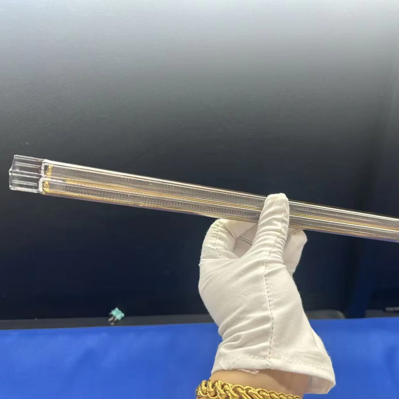
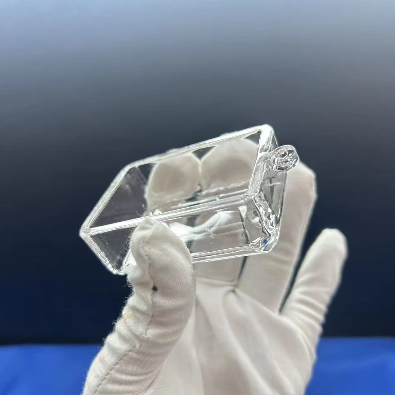
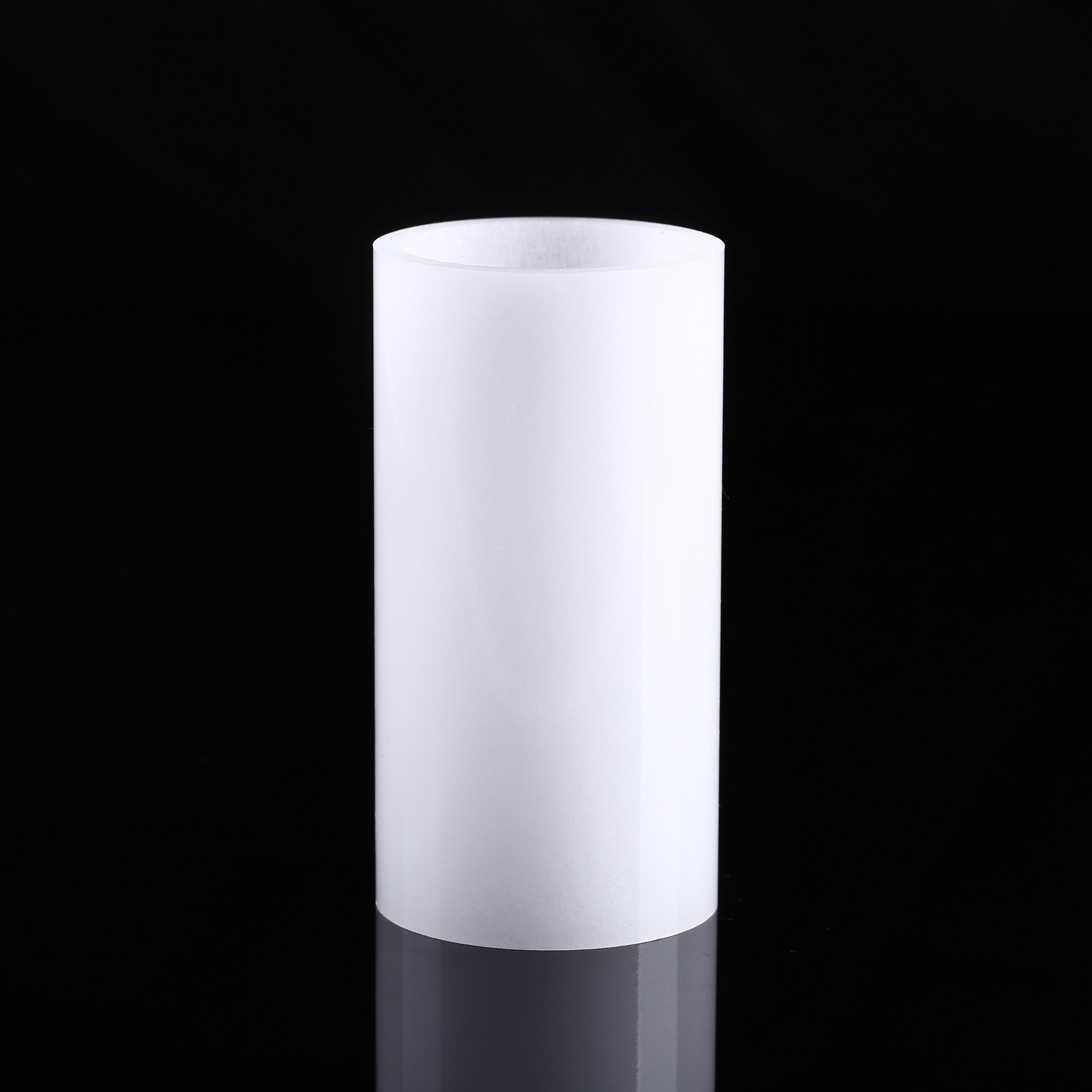
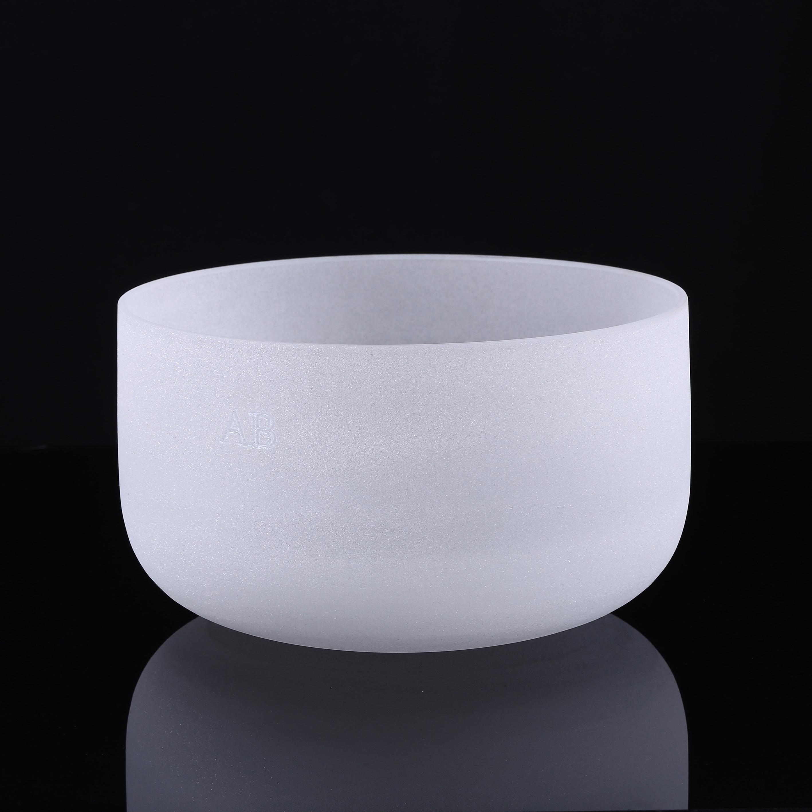
High-Purity Quartz Glass Components for Semiconductor & Lab Workflows

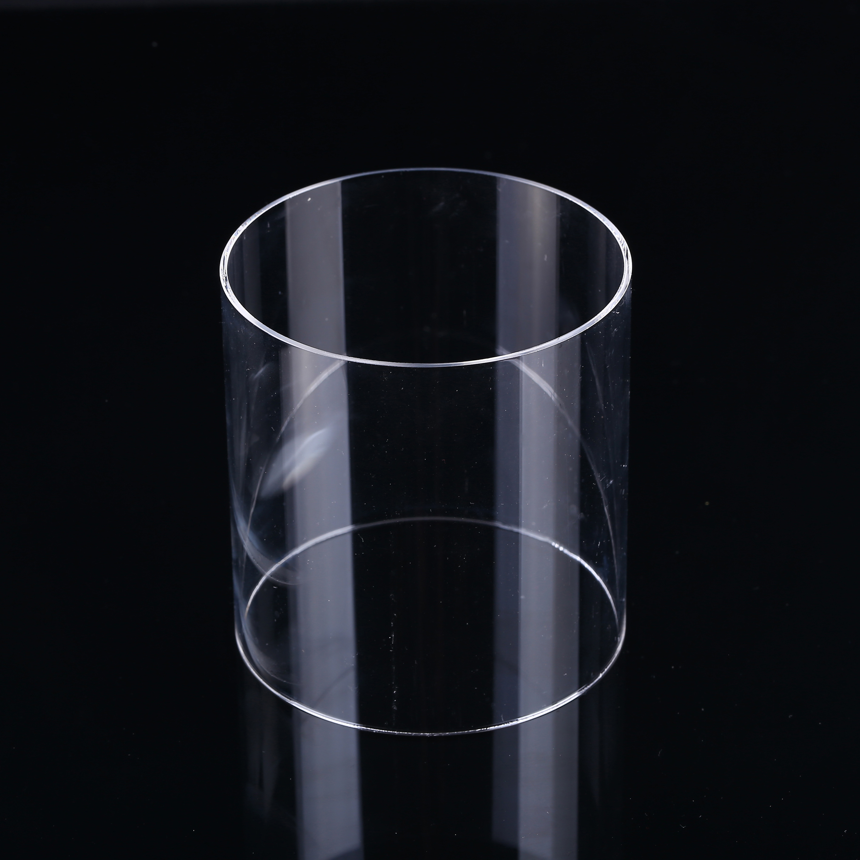
Formulated with high-grade synthetic fused silica and purified natural quartz crystals (SiO₂ purity ≥ 99.995%). Each product is engineered to deliver exceptional thermal stability, corrosion resistance, and optical clarity across high-temperature chemical environments.

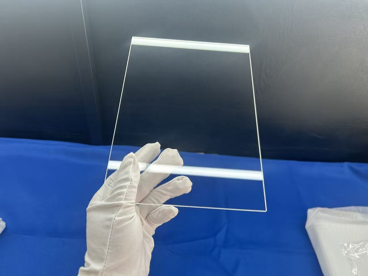
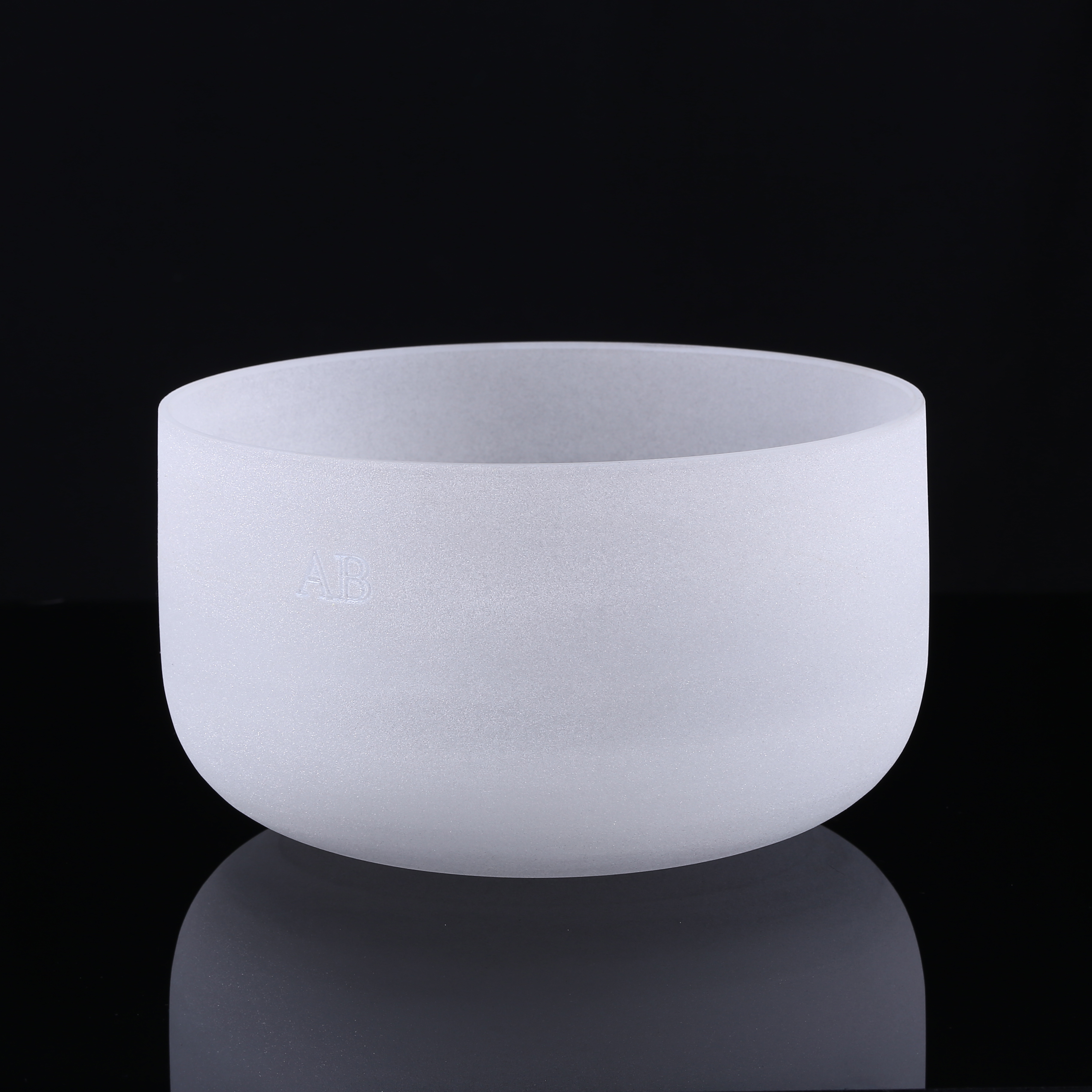
Thermal Shielding Frosted Quartz Sheet for Semiconductor Heating

Frosted Quartz Sheet

Surface-treated quartz plates engineered for uniform infrared heat dispersion, anti-glare sight chambers, and plasma etch baffles. Resists devitrification up to 1150°C.

Executive Industry Analysis

Engineering High-Purity Fused Quartz for Mission-Critical Semiconductor Fabrications

In modern semiconductor manufacturing, fused quartz glass (HPFS - High Purity Fused Silica) serves as an irreplaceable structural and process consumable across the entire wafer fabrication cycle. Operating inside front-end-of-line (FEOL) and back-end-of-line (BEOL) environments, quartz components must withstand sustained processing temperatures exceeding 1100°C while subjected to reactive halogen gas chemistries, violent thermal cycling, and stringent particulate contamination standards. Even minor elemental leaching—measured in parts per billion (ppb)—of heavy metals such as iron (Fe), copper (Cu), or mobile ionic contaminants like sodium (Na) and potassium (K) will cause fatal lattice defects, dielectric breakdown, and degraded wafer yields.

As a specialized high-purity quartz manufacturing center based in Donghai County, Jiangsu—the premier crystalline quartz hub of China—Donghai County Nivra Quartz Products Co., Ltd. integrates raw crystal enrichment, precision mechanical cold processing, CNC ultrasonic milling, and cleanroom fire-polishing. Founded in February 2019, our industrial manufacturing enterprise employs between 101 and 200 skilled glass technicians, optical engineers, and QA specialists dedicated to serving tier-one semiconductor equipment manufacturers (OEMs), solar cell lines, and advanced optical research centers across North America, Europe, and the Asia-Pacific.

The Nivra Quartz Quality Paradigm: By leveraging raw silica pegmatite resources with rigorous chemical purification, our semiconductor furnace components, diffusion tubes, wafer boats, and optical windows maintain an overall chemical purity of 99.995% to 99.999% (SiO₂), ensuring zero structural devitrification, uniform wall thickness, and near-zero coefficient of thermal expansion (5.5 × 10⁻⁷ /°C).
≥99.995%
SiO₂ Chemical Purity Assayed
1683 °C
Softening Point Threshold
≤ 5 Hours
Rapid Engineering RFQ Response
40% / 20%
Exports: North America & Western Europe
Material Science Matrix

Semiconductor Fused Quartz Properties & Grade Selection

Selecting the appropriate quartz grade is essential to balance capital expenditure against operational lifetime, chemical corrosion rates, and optical transmission requirements.

Trace Impurity Element Standard Electric Melt (PPM) Semiconductor Grade Nivra-4N5 (PPM) Synthetic Fused Silica Nivra-5N (PPM) Detection Methodology
Aluminum (Al) 14.0 – 20.0 ≤ 6.00 ≤ 0.05 ICP-MS
Iron (Fe) 0.80 – 1.50 ≤ 0.15 ≤ 0.02 ICP-MS
Titanium (Ti) 1.00 – 1.80 ≤ 0.80 ≤ 0.01 ICP-MS
Calcium (Ca) 0.70 – 1.20 ≤ 0.40 ≤ 0.02 ICP-MS
Sodium (Na) 1.00 – 2.00 ≤ 0.30 ≤ 0.01 AAS
Potassium (K) 0.80 – 1.60 ≤ 0.30 ≤ 0.01 AAS
Lithium (Li) 0.50 – 1.00 ≤ 0.20 ≤ 0.01 AAS
Hydroxyl Group [OH⁻] < 5 – 30 < 15 (Standard Annealed) < 1000 (UV) / < 5 (Low-OH) FTIR Absorption

JGS1: Synthetic Fused Silica

Synthesized via vapor phase hydrolysis of SiCl₄. Possesses outstanding transmittance from deep ultraviolet (DUV 185 nm to 2500 nm), free of bubbles and inclusions. Recommended for stepper lithography lenses, laser windows, and UV cuvettes.

JGS2: Optical Fused Quartz

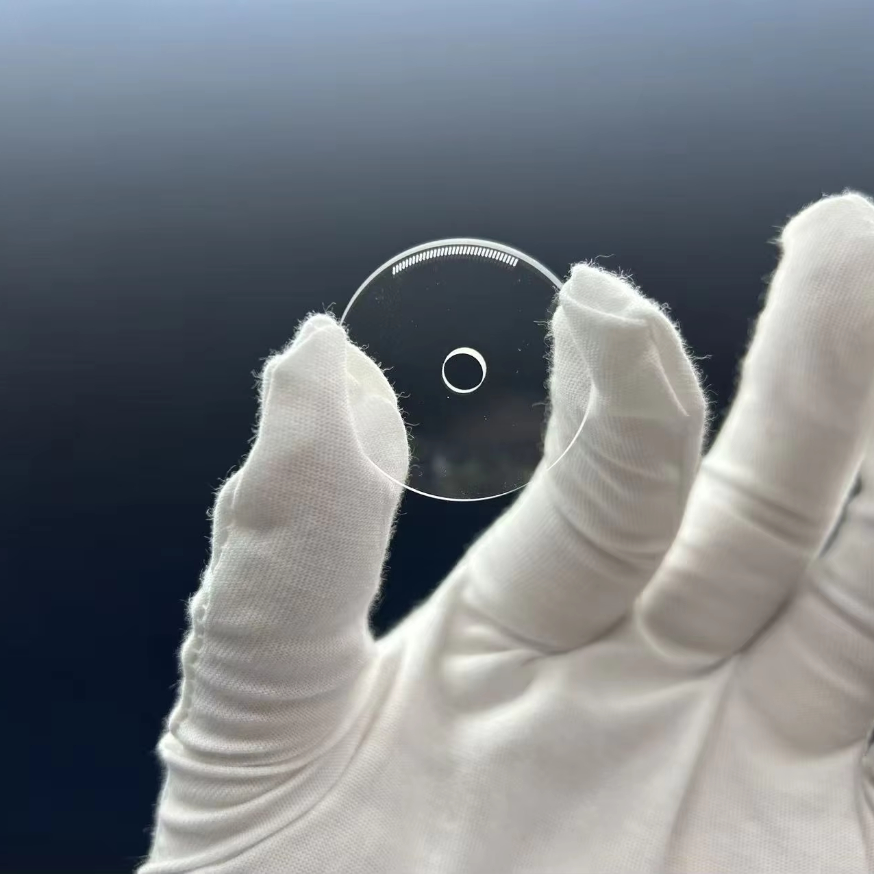
Produced through continuous electric melting of pure natural crystal quartz sands. Transmits cleanly from 220 nm to 2500 nm. Preferred industry choice for wafer observation viewports, sight glasses, furnace flanged manifolds, and high-temperature optical discs.

JGS3: Infrared Grade Quartz

Vacuum-melted fused quartz with trace hydroxyl content ([OH⁻] < 2–5 ppm). Eliminates the characteristic 2.73 μm absorption dip, maximizing IR transmission from 260 nm to 3500 nm. Ideal for pyrometer viewports, epitaxial wafer heating, and FTIR optics.

Strategic Procurement Intelligence

Future Sourcing & Procurement Trends in Semiconductor Quartz (2025–2030)

Global supply chain adjustments, sub-3nm chip production architectures, and shifting raw mineral availability are fundamentally reshaping how procurement executives source fused quartz.

1. Accelerated Shift to Synthetic Silica in Critical Plasma Etch Zones

As design rules drop below 3nm, conventional natural fused quartz rings and showerheads suffer subtle grain erosion under aggressive CF₄/NF₃ plasma chambers. High-purity synthetic quartz with uniform network density is increasingly required by procurement directors to curb micro-particle detachment and double component chamber lifetimes.

2. Large-Format Scaling for 300mm/450mm Vertical Batch Furnaces

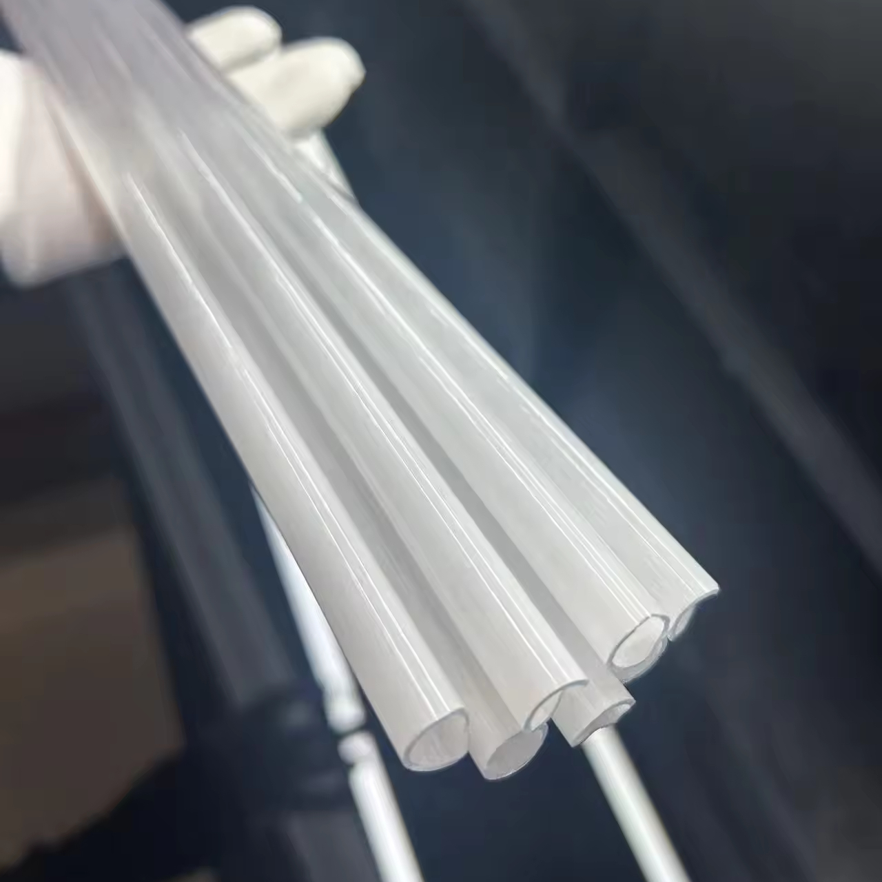
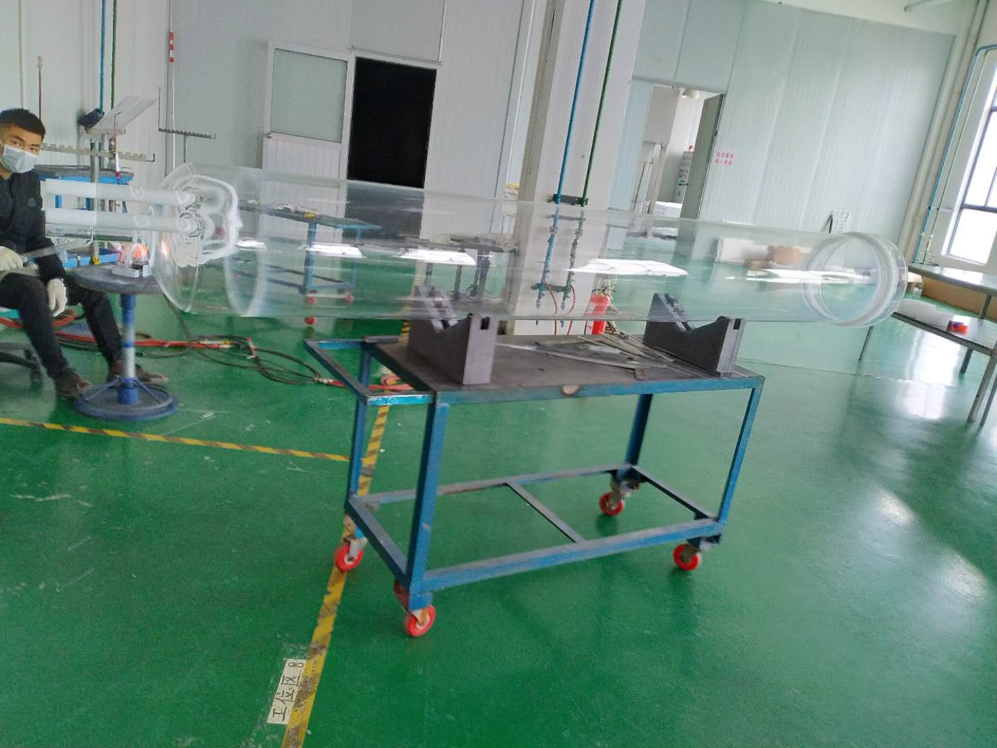
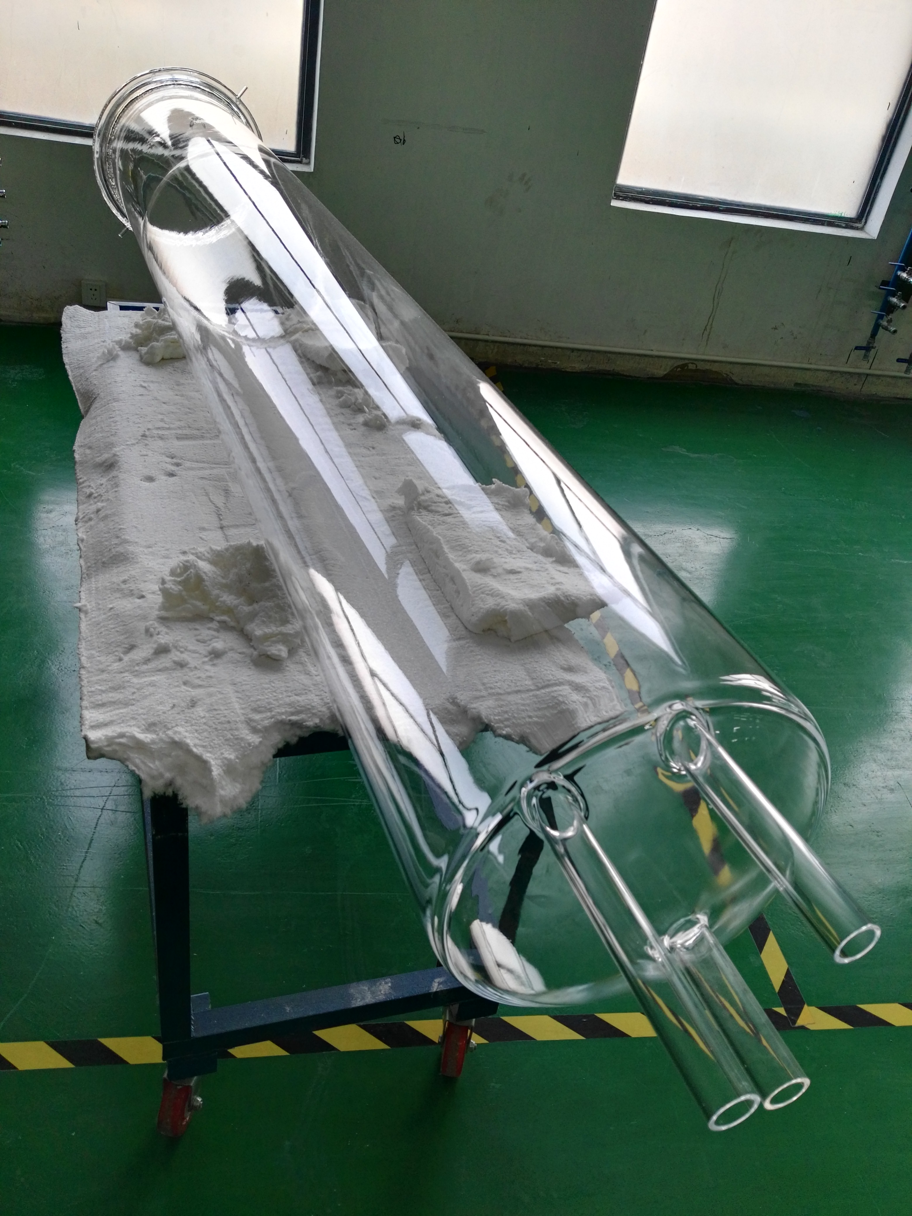
Fab expansions require quartz furnace process tubes with inner diameters reaching 400mm–550mm and lengths over 2.4 meters. Sourcing trends prioritize suppliers capable of maintaining strict outer diameter tolerances (±0.3mm), wall uniformity, and low warp over thermal campaigns without sagging or micro-cracking at flame welded joints.

3. Rigorous Trace Element Auditing and Direct Manufacturer Transparency

Procurement teams are cutting through multi-tiered broker layers to secure direct relationships with integrated Chinese manufacturers. Full lot traceability, batch ICP-MS chemical reports, and live cleanroom verification audits are becoming standard requirements to mitigate cross-border supply chain volatility.

R&D Roadmaps

Fabrication Technological Trends & Next-Gen Glass Processing

Discover how innovative manufacturing processes are overcoming thermal devitrification, mechanical stress, and micro-dimensional drift.

5-Axis CNC Ultrasonic Milling

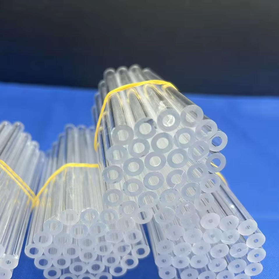
Non-contact ultrasonic micro-machining prevents sub-surface micro-cracks in quartz wafers, high-slot wafer boats, and slotted flanges, ensuring dimensional repeatability within ±0.01mm.

Plasma Flame Polishing & Annealing

Thermal stress relief via computerized vacuum annealing furnaces at 1180°C eliminates residual stresses induced during cold grinding, completely eradicating spontaneous shattering risks.

Anti-Devitrification Coatings

Novel surface dopants and thermal conditioning protocols suppress cristobalite nucleus formation at elevated temperatures, prolonging quartz crucible and furnace muffle lifespans by up to 35%.

Zero-Bubble Fusion Welding

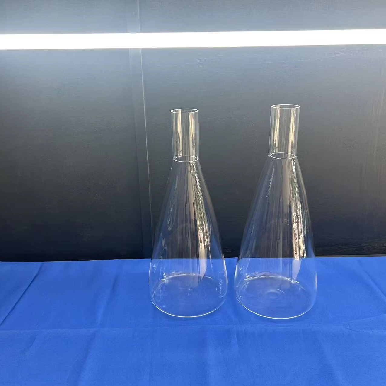
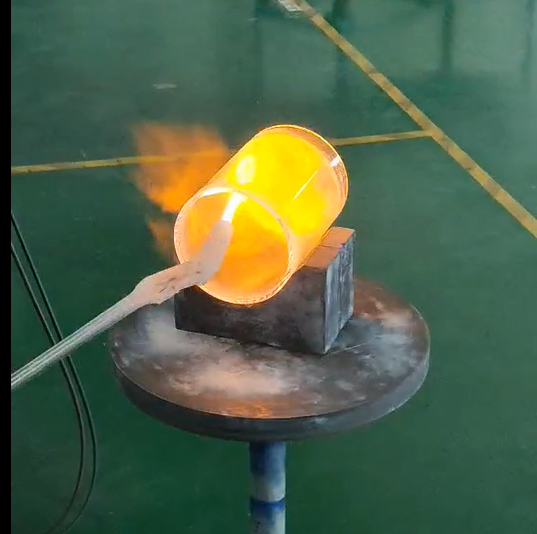
Hydrogen-oxygen lathe fusion allows joining of intricate quartz manifolds, bell jars, and bubblers with microscopic seam integration, preventing particulate traps during wafer wash sequences.

Manufacturer Credentials

Why Tier-1 Semiconductor Buyers Source from Nivra Quartz

Headquartered at 285 Heping East Road, Lianyungang, Jiangsu, Nivra Quartz combines raw geographic supply advantages with modern cleanroom glass fabrication technologies.

Donghai Origin Hub

Located right in Donghai County—the crystal center of China. Direct access to premium silica sources guarantees steady supply, stable prices, and low raw material lead times.

Integrated OEM/ODM Chain

From CAD/STEP drawing engineering review to raw cylinder drawing, CNC slotting, laser cutting, optical polishing, and cleanroom vacuum packaging—every step is handled in-house.

≤ 5h Inquiry Response

Our dedicated technical sales engineers deliver rapid quotation turnarounds and drawing feasibility analyses with a measured 88.89% responsive interaction rating.

Global Export Packaging

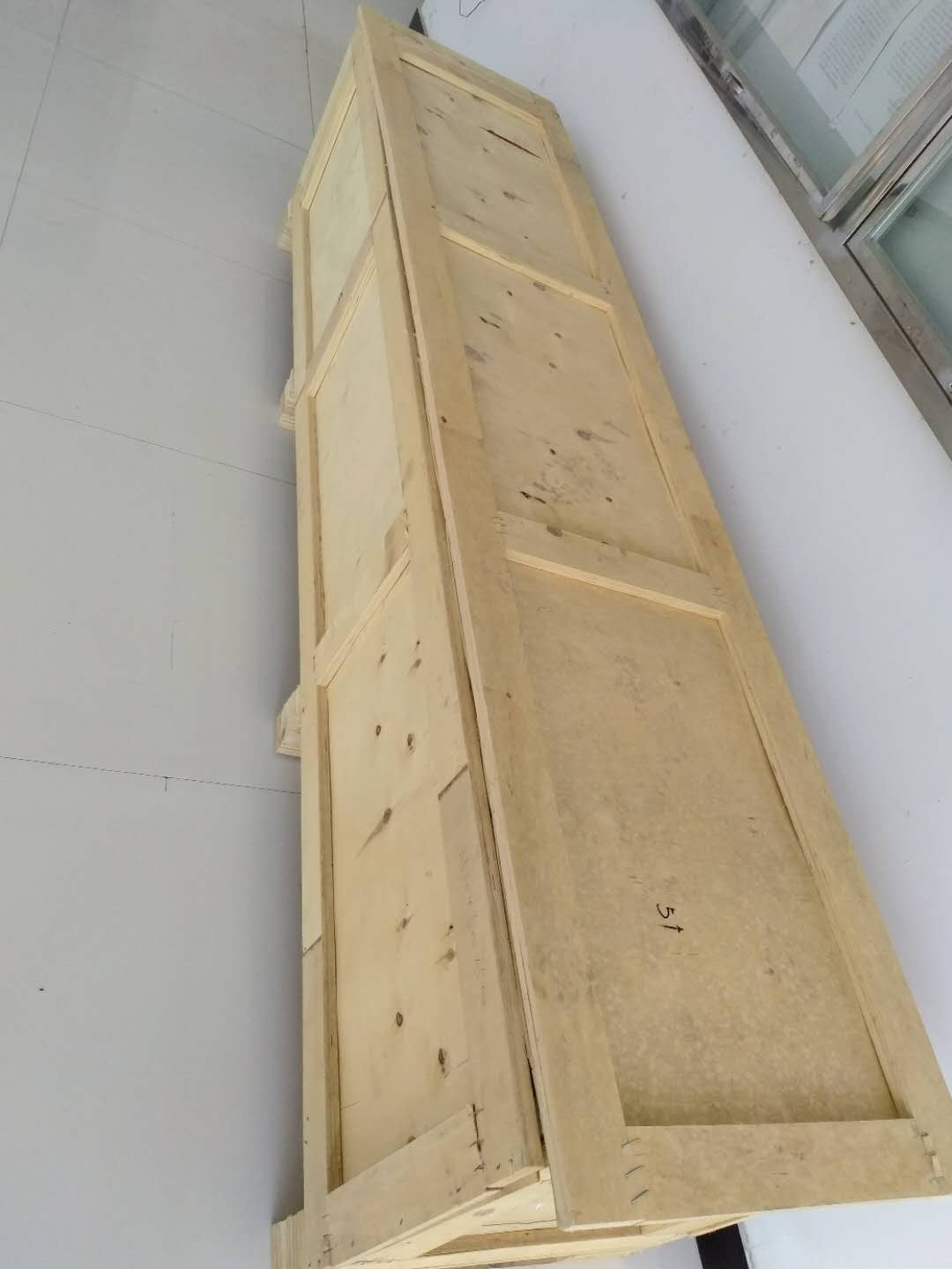
Custom multi-layer suspended foam liners, vacuum moisture bags, and reinforced non-fumigation wooden export crates ensure 100% zero-breakage delivery to overseas cleanrooms.

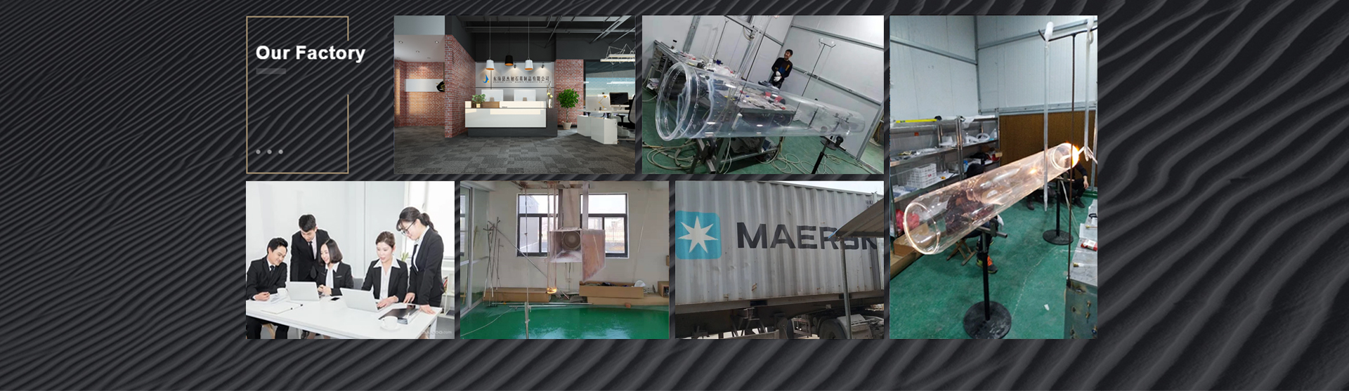
Quartz Glass Machining and Lathe Forming Workshop
Thermal Flame Lathe & Forming Workshop
Precision CNC Quartz Grinding and Cold Working
High-Precision CNC Cutting & Grinding Line
Cleanroom Final Inspection and Optical Measurement
Cleanroom Inspection & Safe Export Packaging
Finished Semiconductor Quartz Products
Semiconductor Flanges, Discs & Crucible Storage

Verified On-Site Compliance & Qualification Documents

Nivra Quartz Business Registration Document
Quality Compliance Audit Certificate
Export Business Verification Document
Material Testing Qualification Report
Procurement Guidance

Frequently Asked Questions: Sourcing Semiconductor Fused Quartz

Detailed engineering answers covering purity grades, thermal thresholds, custom tolerances, and overseas shipping logistics.

How do you prevent devitrification of quartz furnace tubes during prolonged high-temperature runs?
Devitrification—the phase transformation of amorphous fused silica into crystalline cristobalite—initiates around 1150°C and accelerates in the presence of alkali metal surface contaminants (such as Na, K, Ca, or fingerprint grease). Nivra Quartz addresses this through two protocols: first, maintaining total alkali impurities below 0.8 ppm; second, applying a rigorous hydrofluoric (HF) acid cleaning and high-purity deionized water ultrasonic wash prior to annealing. For fab operators, we recommend cleanroom handling with lint-free gloves and periodic 5% HF etching to strip surface micro-nucleation sites.
What geometric tolerances can your CNC ultrasonic machining achieve on wafer boats and slotted discs?
For standard semiconductor furnace boats, quartz wafer carriers, and custom slotted discs, our 5-axis CNC ultrasonic workstations achieve slot width and pitch tolerances within ±0.03mm. Overall length and diameter tolerances on tubes are held to ±0.2mm, while wall thickness variations can be calibrated within ±0.1mm. Precision optical plates and wafers achieve optical parallelism under 10 arcseconds with surface flatness reaching λ/4 or better.
What are the differences between JGS1, JGS2, and JGS3 fused quartz grades?
JGS1 is synthetic fused silica engineered from silicon tetrachloride (SiCl₄), optimized for deep-ultraviolet (DUV) applications from 185 nm to 2500 nm with negligible bubble and inclusion density.
JGS2 is optical-grade fused quartz manufactured from electric-fused natural quartz crystals, providing transmission from 220 nm to 2500 nm, suited for general optical windows, sight glasses, and viewport plates.
JGS3 is infrared-grade fused silica processed to minimize hydroxyl content ([OH⁻] < 5 ppm), eliminating the 2.73 μm absorption peak to achieve smooth infrared transmission up to 3500 nm.
What continuous and peak operating temperatures can your fused quartz components endure?
Our clear fused quartz products operate continuously at 1100°C without dimensional deformation. They withstand short-term peak thermal exposures up to 1450°C. The softening point of our material is approximately 1683°C, while the annealing point is 1215°C. Due to an extremely low coefficient of thermal expansion (5.5 × 10⁻⁷ /°C), our components can withstand direct quenching from 1000°C into ambient cold water without fracture.
Can you manufacture custom quartz labware directly from our CAD, STEP, or PDF engineering drawings?
Yes. Custom OEM and ODM fabrication forms the core of our business. We routinely process complex customer geometries provided in STEP, DWG, DXF, or detailed PDF formats. Our engineering team conducts full design for manufacturability (DFM) reviews within 5 hours, offering suggestions on wall transitions, welding seams, and cost-effective raw tube blank selection.
What are your typical minimum order quantities (MOQs) and prototype lead times?
For standard catalog items, furnace process tubes, crucibles, and large tanks, our MOQ starts from 1 to 5 pieces to support engineering R&D and tool evaluations. Smaller precision optical discs and micro-wafers usually carry an MOQ of 50 to 100 pieces. Prototype orders are typically fabricated, inspected, and dispatched within 7 to 10 working days.
How does Nivra Quartz ensure zero breakage during international air and sea shipping?
Fragile quartz ware is packaged using high-density polyethylene (EPE) shock-absorbing contoured foam molds, vacuum anti-static inner poly-bags, and heavy-duty double-corrugated export cartons. For heavy tubes, tanks, and crucibles, outer packaging consists of reinforced, fumigation-free plywood crates built with internal shock suspension ribs. Over our multi-year export history across 43+ transactions, our damaged-in-transit rate is below 0.05%.
Direct Factory Engineering Support

Accelerate Your Semiconductor Quartz Sourcing Project

Whether you require replacement 300mm diffusion tubes, high-volume wafer carrier boats, custom laser windows, or welded wet cleaning tanks, our Donghai engineering team provides responsive technical guidance, direct-factory pricing, and rigorous material traceability.