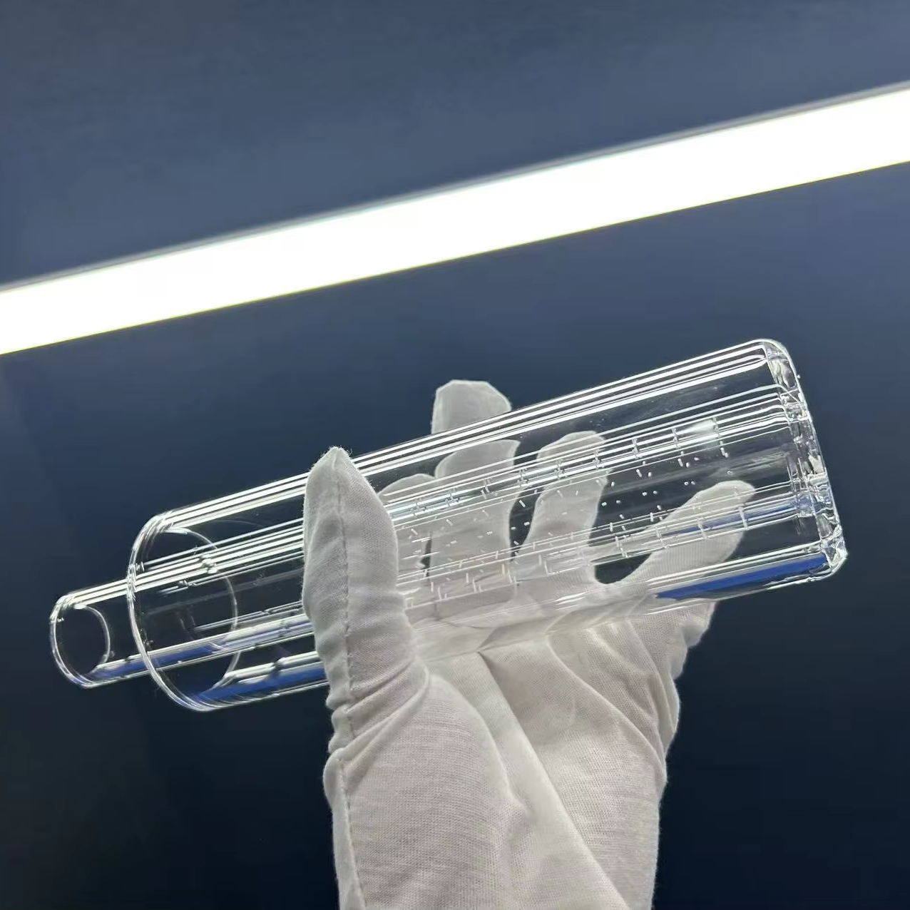
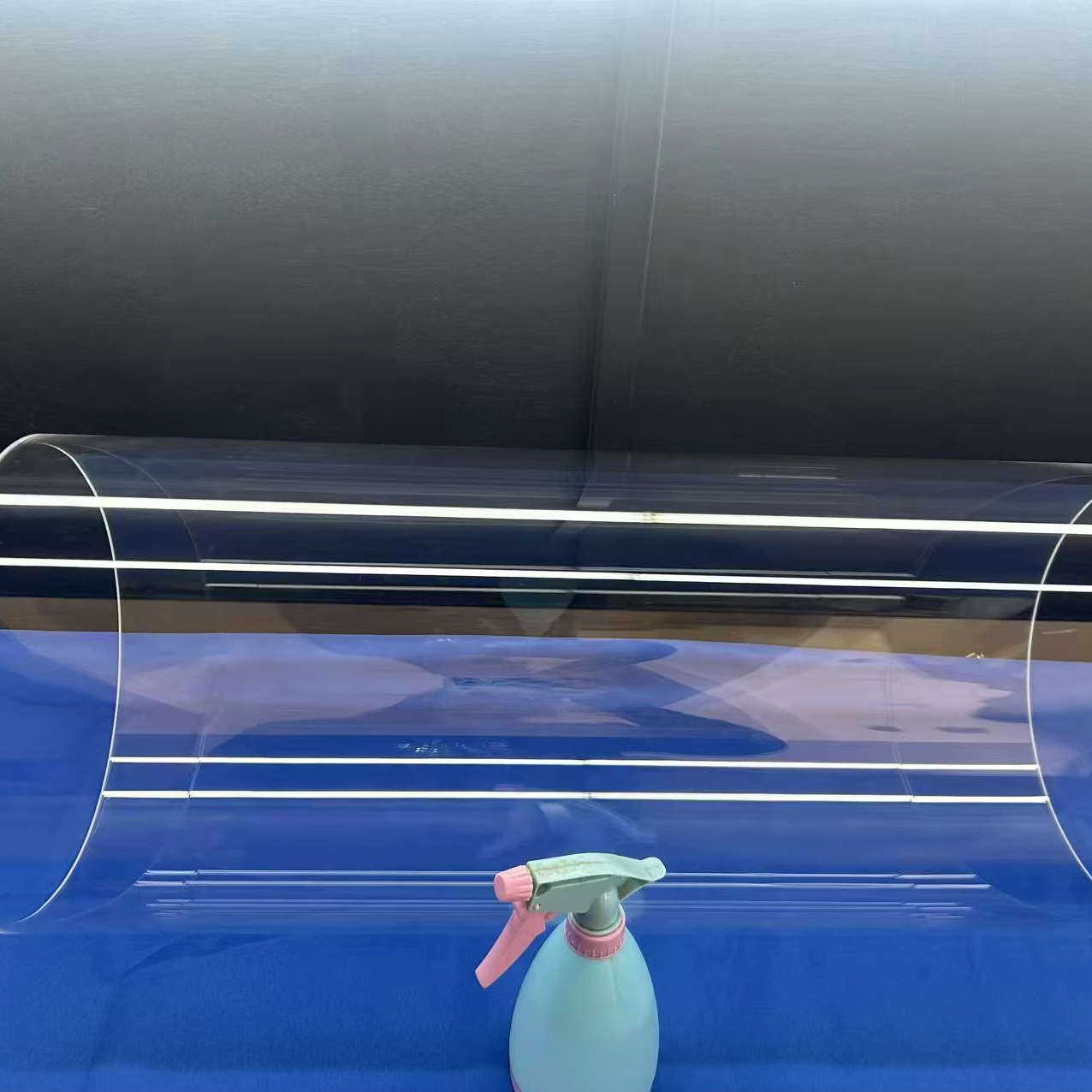
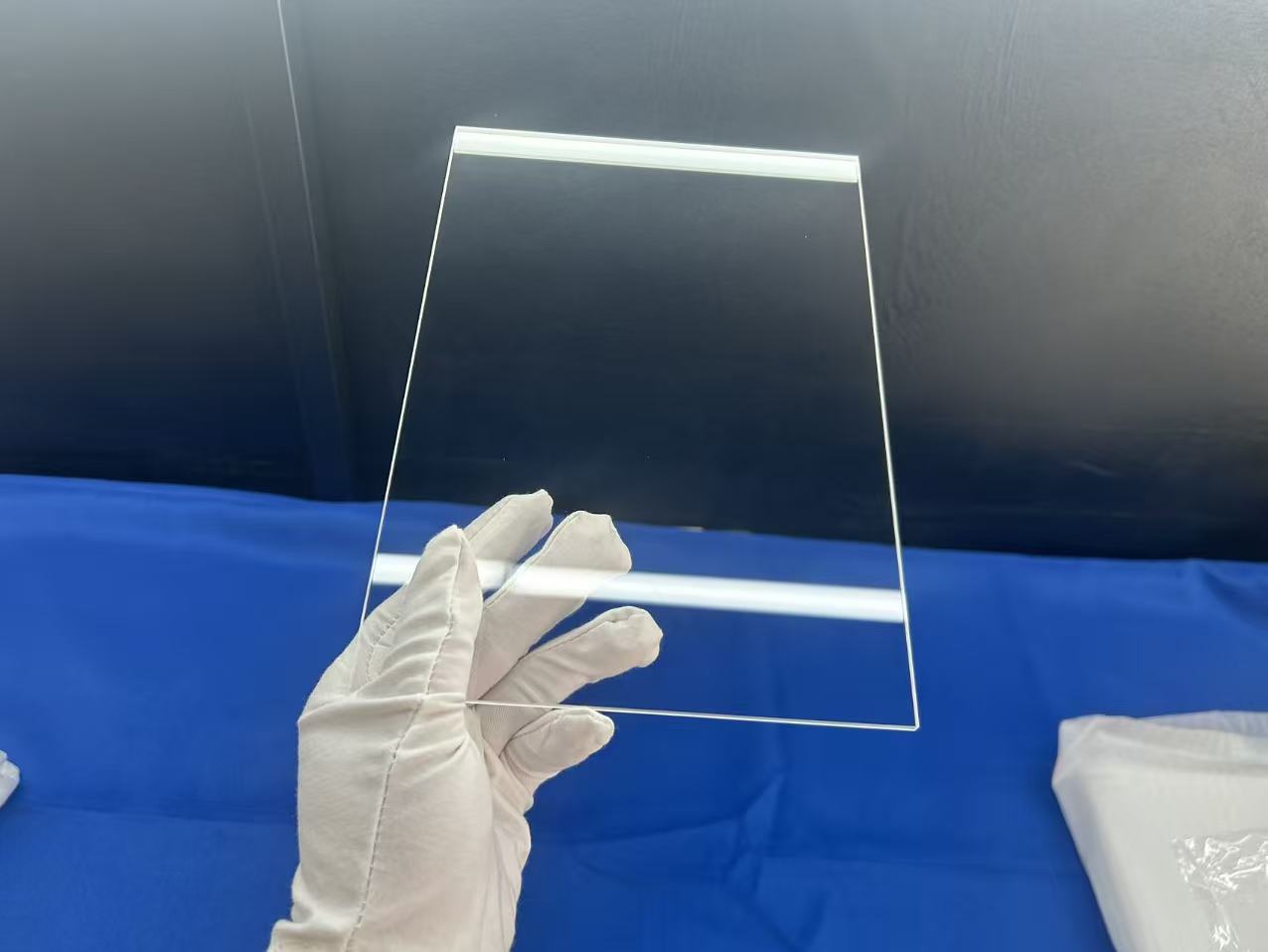
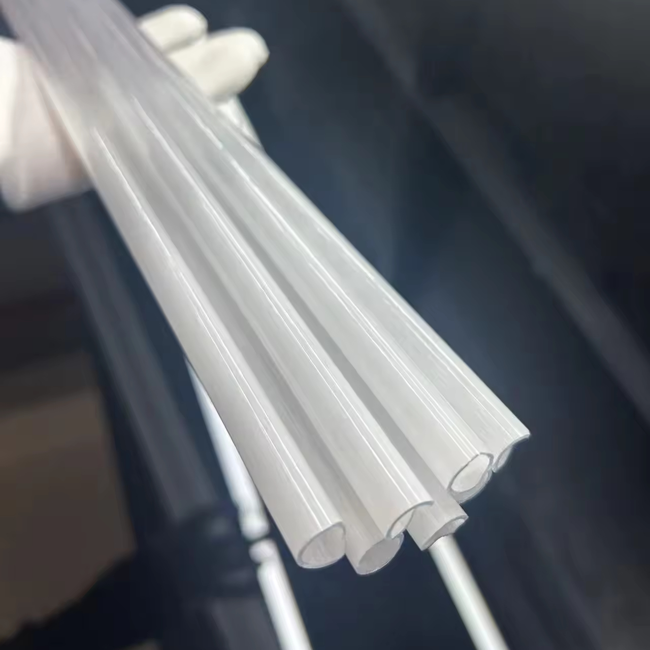
Factory Precision-Machined Quartz Substrates & Components
Fabricated from natural crystalline quartz and chemical synthetic quartz (JGS1, JGS2, JGS3). Every substrate undergoes strict interferometric inspection, laser edge profiling, and multi-stage ultrasonic degreasing prior to Class 100 packaging.
Rooted in Donghai, China's Silicon Capital
In-house CNC, polishing, flame-welding teams
88.89% rapid quotation & drawing review
40% North America, 34% Europe verified share
Structural Metallurgy & Optical Physics of Synthetic vs. Fused Quartz Substrates
Understanding the atomic lattice disparities, dielectric behavior, and optical dispersion factors between electric-arc fused natural quartz and chemical vapor deposited (CVD) synthetic silica.
| Standard Grade | Precursor / Method | Transmission Spectrum | Hydroxyl (OH⁻) Conc. | Typical Semiconductor / Optical Application |
|---|---|---|---|---|
| JGS1 (Far UV) Deep UV | Synthetic CVD Silicon Hydrolysis | 185 nm – 2500 nm | High (800 – 1200 ppm) | EUV/DUV mask blanks, excimer laser windows, lithography wafer carriers |
| JGS2 (Optical Grade) UV-VIS | Refined Natural Quartz (Oxy-hydrogen) | 220 nm – 2500 nm | Medium (150 – 300 ppm) | Optical instrument windows, sight glasses, solar wafer carrier boats |
| JGS3 (Infrared Grade) IR-Vacuum | Electric Vacuum Melting | 260 nm – 3500 nm | Ultra-low (< 2 – 5 ppm) | Infrared pyrometry, thermal analysis shields, high-power CO₂ laser lenses |
| Semiconductor Fused Silica | Continuous Electrically Fused Ingot | Visible to Near-IR | < 30 ppm | Diffusion furnace core liners, wafer boats, plasma etching chamber rings |
Critical Fabrication Metrics: Surface Metrology & Defect Classification
Understanding the stringent parameters governing modern wholesale procurement: Total Thickness Variation (TTV), wavefront distortion, and MIL-PRF-13830B surface cosmetic standards.
Roughness (Ra < 0.2 nm)
Achieved through double-sided Chemical Mechanical Polishing (CMP) utilizing nano-cerium oxide slates, eradicating scattering centers for ultra-high power laser and EUV bounce optics.
Flatness & TTV (< 1 µm)
Interferometrically verified transmitted wavefront error ($\lambda/10$ to $\lambda/20$ at $632.8\text{ nm}$). Low Total Thickness Variation guarantees uniform thermal conductive transfer during CVD depositions.
Scratch-Dig (10/5 – 20/10)
Adheres to MIL-PRF-13830B and ISO 10110 standards. Zero micro-cracks along CNC waterjet or diamond-beveled chamfers (C-shape or R-profile) prevents catastrophic fracture propagation under high thermal shock.
Purity & Laser Damage
Trace metallics verified by Inductively Coupled Plasma Mass Spectrometry (ICP-MS) ($Fe, Na, K, Li, Ca < 0.05\text{ ppm}$). Laser Induced Damage Threshold (LDT) exceeds $15\text{ J/cm}^2$ @ $1064\text{ nm}, 20\text{ ns}$.
Global Quartz Substrate Procurement Trends (2025–2030)
As semiconductor fabrication scales sub-2nm nodes and photonics convergence transforms computing architectures, procurement executives are adjusting their sourcing models from simple standard catalog orders to specialized structural co-development.
1. Glass Core Substrates & TGV Interposers
Traditional organic packaging substrates are reaching mechanical and dielectric limitations in high-performance computing (HPC) and AI accelerators. High-purity quartz and borosilicate glass core substrates featuring laser-drilled Through Glass Vias (TGV) offer zero warpage, stellar dielectric constants ($Dk \approx 3.8$), and ultra-low loss tangents ($Df < 0.002$ at $10\text{ GHz}$), allowing denser interconnects and superior signal fidelity.
2. Direct Sourcing from Donghai Clusters
Global supply chain leaders in the US and Europe are actively consolidating their vendor bases by bypassing intermediate trading houses and contracting directly with vertically integrated foundries in Donghai County. Controlling the flow from crude silicon reduction to finished 5-axis CNC diamond grinding lowers production costs by 30% to 45% while ensuring rapid prototyping iteration cycles.
3. Ultra-Clean & Anti-Contamination Protocols
With the rapid expansion of 300mm wafer fabrication in power electronics (SiC, GaN epitaxy) and solar photovoltaics (TOPCon, HJT cells), wafer carrier trays and quartz boats face intense exposure to reactive plasma etch cycles. Buyers prioritize quartz substrates synthesized with ultra-dense crystalline grain structures that curb particulate flake generation and ensure long operating lives in chlorine/fluorine atmospheres.
4. Ultrafast Laser & Precision Micro-Machining
Conventional mechanical diamond-core drilling frequently introduces micro-fissures and edge spallation. The procurement baseline is shifting to cold picosecond and femtosecond laser micromachining. Laser Induced Deep Etching (LIDE) achieves ultra-precise non-tapered holes, micro-fluidic channels, and complex geometries with sub-micron edge definition, drastically increasing mechanical fracture strength.
OEM/ODM Seamless Engineering Procurement Roadmap
A rigorous, five-phase transition model engineered to support foreign procurement divisions from initial rapid CAD reviews to certified bulk deliveries.
Requirement & CAD Evaluation
Upload your 2D/3D models (STEP, DWG, DXF, PDF). Our engineering staff completes DFM (Design for Manufacturability) analysis, confirming optimal quartz grade (JGS1/2/3), optical tolerances, and thermal parameters within 5 hours.
Precision CNC & CMP Processing
From initial continuous-cast ingot slicing to dual-sided lapping, diamond chamfering, and chemical mechanical planarization, all workflows take place under strict ISO 9001:2015 process controls to maintain flawless dimension stability.
Interferometry & Cleanroom Packing
Parts undergo Zygo laser interferometry, spectrophotometric transmission mapping, ultrasonic multi-solvent wash baths, and cleanroom vacuum foil sealing inside drop-tested, fumigation-free wooden export crates.
Why International Tier-1 Buyers Choose Nivra Quartz
Headquartered at 285 Heping East Road, Lianyungang, Jiangsu, Donghai County Nivra Quartz Products Co., Ltd. combines localized mineral refining dominance with rigorous industrial manufacturing management.
Donghai Silicon Hub Advantage
Donghai accounts for over 70% of China's quartz extraction and advanced fused silica refining. Our geographic location gives us unhindered access to raw crystal ingots, ensuring exceptional batch-to-batch consistency and competitive pricing across high-volume production orders.
101-200 Specialized Craftsmen
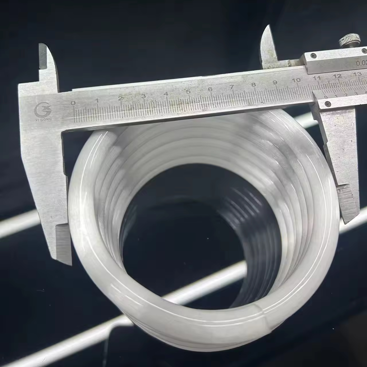
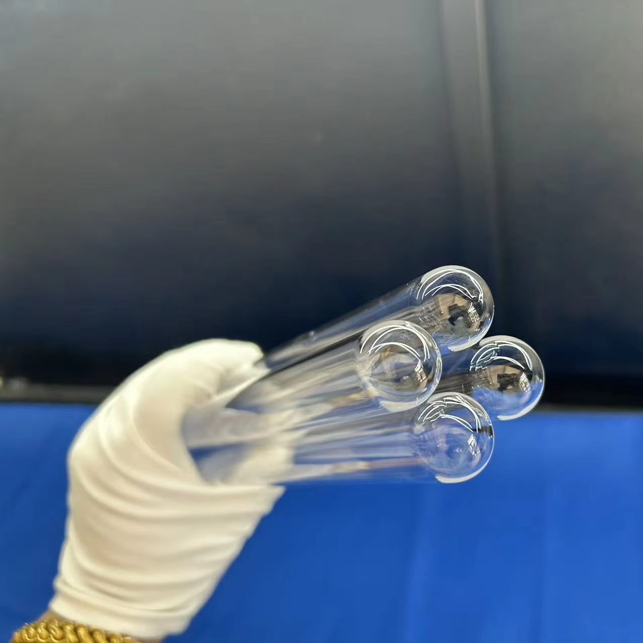
Operating modern CNC milling centers, optical double-disc polishing machinery, and multi-axis glass-blowing lathes, our technicians weld, flame-fire, shape, and inspect critical custom components—from helical quartz coils to 450mm diameter diffusion furnace tubes.
Rapid Engineering Turnaround
With an independently verified inquiry response rate of 88.89% and average initial engineering replies completed within 5 hours, we drastically accelerate prototyping schedules for fast-paced semiconductor, medical, and aerospace R&D teams.
Verified Export Track Record
Maintaining a flawless 5.0/5.0 buyer satisfaction score with repeated contract fulfillment across 40+ countries. Consistently preferred by procurement heads in North America (40%), Western Europe (20%), and Eastern Europe (14%) for our exceptional packing and documentation integrity.
Frequently Asked Questions on Quartz Substrate Sourcing
Addressing critical engineering concerns, quality assurance standards, shipping contingencies, and material grade determinations.
What are the key technical differences between JGS1, JGS2, and JGS3 quartz substrates?
JGS1 (Synthetic Fused Silica) is produced through the synthetic vapor-phase flame hydrolysis of silicon halides ($SiCl_4$). It features zero seed/bubble inclusion, extreme purity (total metallic impurities < 0.1 ppm), and transmits exceptionally well across the vacuum-ultraviolet spectrum down to 185 nm. It is the premier choice for excimer laser photolithography, UV spectrometer cuvettes, and optical mask blanks.
JGS2 (Optical Grade Fused Quartz) is melted from high-grade natural refined quartz gravel in hydrogen-oxygen flames. It transmits across the 220 nm to 2500 nm band with excellent mechanical rigidity and low thermal expansion, serving as the commercial standard for optical sight windows, laser protection plates, and standard laboratory instruments.
JGS3 (Infrared Fused Silica) is electric-vacuum-furnace melted from selected natural quartz. It possesses an extremely low hydroxyl group content ($[OH^-] < 2\text{ to }5\text{ ppm}$), effectively eliminating the destructive absorption trough situated at 2720 nm. It transmits seamlessly into the near-to-mid infrared spectrum up to 3500 nm, making it indispensable for infrared cameras, thermal sensors, and high-energy laser optic windows.
How do you manage thermal shock parameters and mechanical stress relief during fabrication?
Due to its exceptionally low thermal expansion coefficient ($\approx 5.5 \times 10^{-7}/\text{°C}$), fused quartz can readily survive immediate quench shocks exceeding $1000\text{°C}$ into ambient water without structural failure. However, heavy CNC grinding, ultrasonic milling, and oxy-hydrogen flame welding inherently introduce localized internal stresses.
To eliminate this residual birefringence, every precision component undergoes thermal annealing in programmed electric kilns. Parts are brought to the annealing zone ($1140\text{°C}$ to $1200\text{°C}$), soaked to equalize the internal thermal gradients, and cooled at precisely managed rates (e.g., $1\text{°C to }3\text{°C}/\text{min}$) down past the strain point ($1070\text{°C}$). Residual stress birefringence is validated with polariscopes to comply with ISO 10110-4 optical limits.
What are the achievable surface flatness and roughness tolerances for custom square plates?
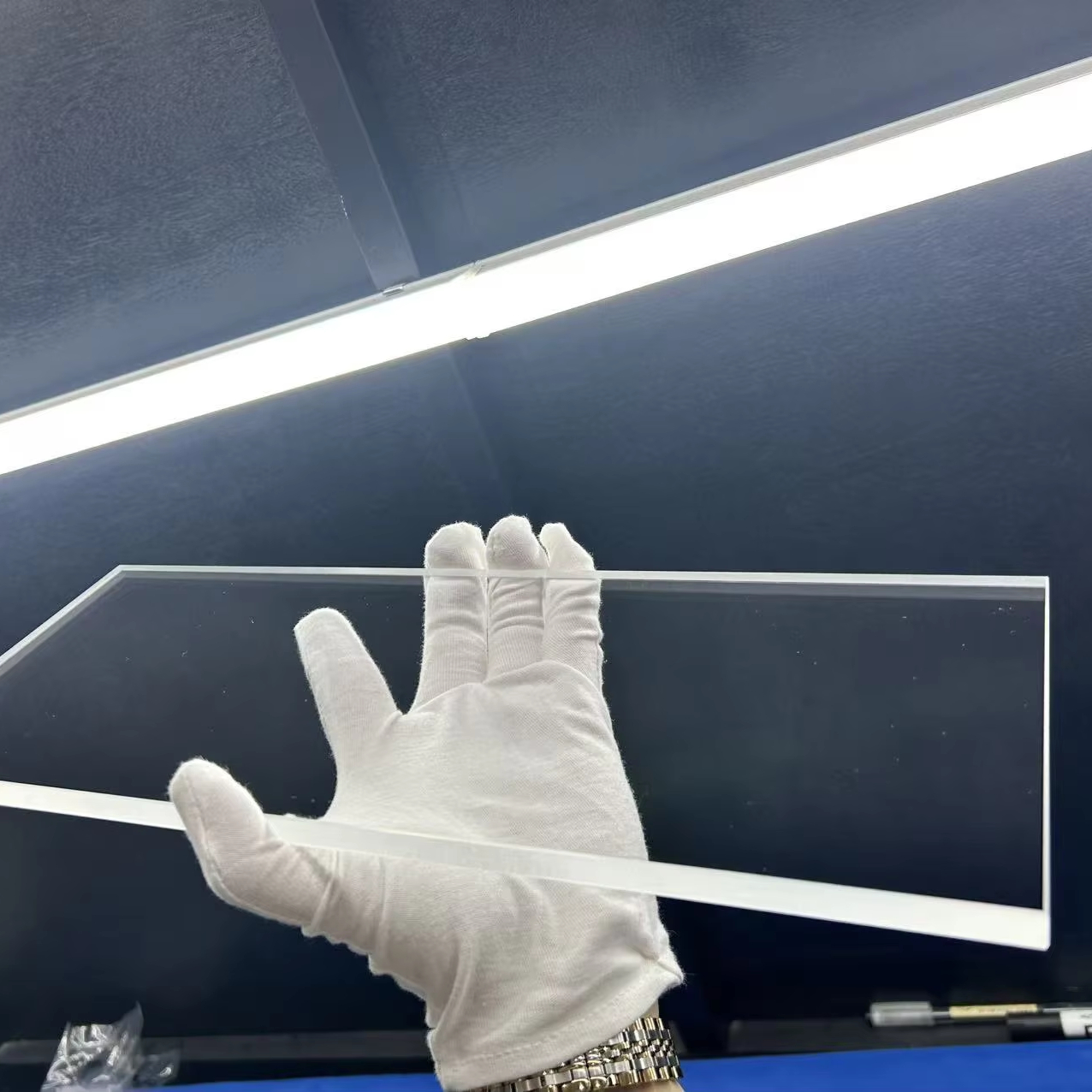
For standard industrial furnace and sight-glass applications, standard mechanical polishing yields a surface roughness of $Ra \approx 0.8 - 1.2\text{ nm}$ with flatness of $2-4\lambda$ per inch.
For high-end semiconductor wafer substrates and precision laser optics, our facility executes double-sided Chemical Mechanical Polishing (CMP) utilizing colloidal silica or high-purity cerium oxide slurries. We regularly achieve a sub-nanometer surface roughness of $Ra < 0.2\text{ nm} - 0.5\text{ nm}$, surface flatness to $\lambda/10$ to $\lambda/20$ at $632.8\text{ nm}$, parallelism under 5 arcseconds, and scratch-dig cosmetic standards of 20/10 or 10/5 per MIL-PRF-13830B.
What Minimum Order Quantities (MOQ) and lead times apply for custom engineered designs?
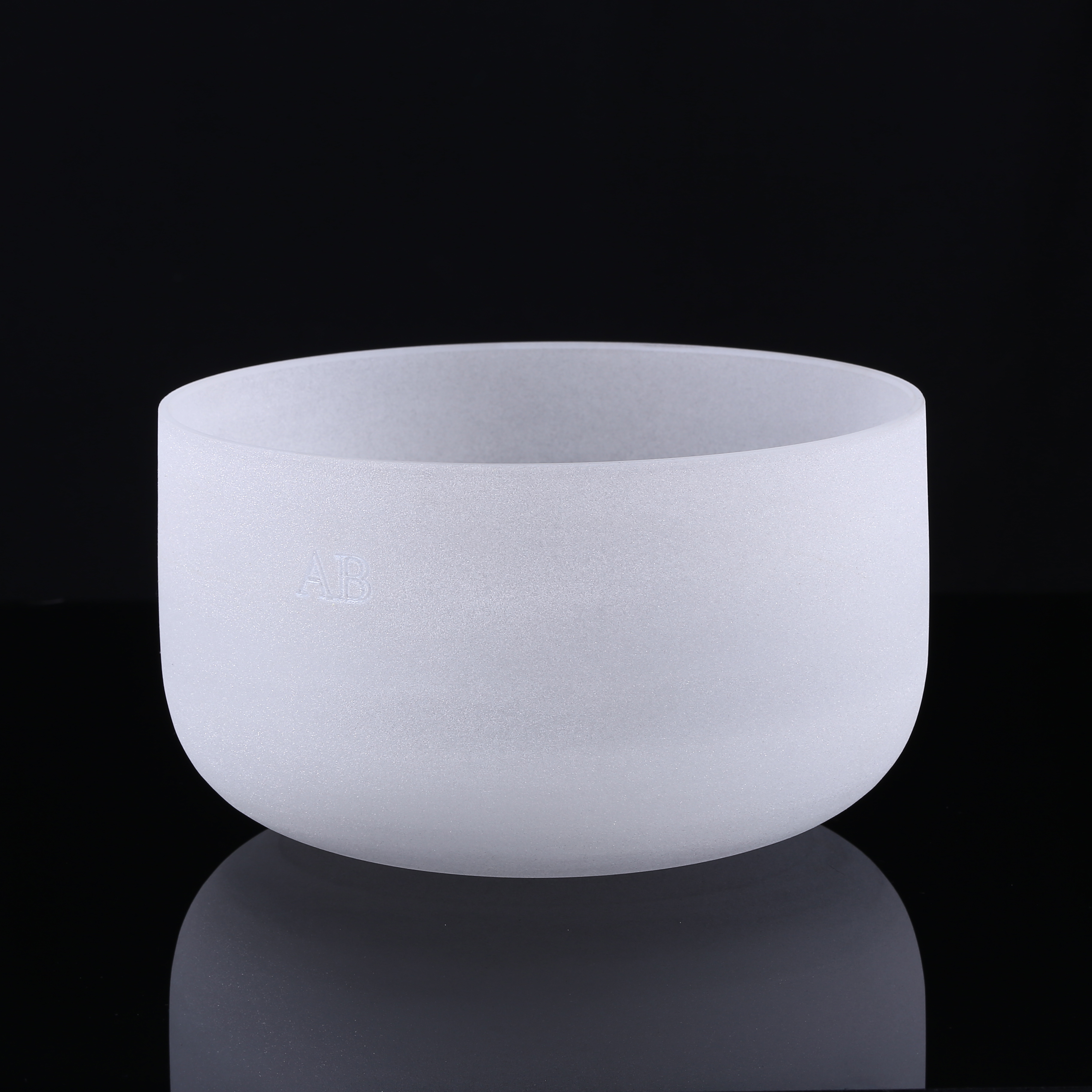
To support prototyping and low-volume pilot runs, we provide highly flexible MOQ tiers: standard tubes, crucibles, and optical discs can be procured with an MOQ of just 1 to 10 pieces. Miniature precision-polished laser windows and customized perforated wafer discs typically carry an entry MOQ of 50 to 100 pieces.
Standard lead times for custom CNC prototyping range from 5 to 10 business days. Large-scale volume production runs (1,000+ pieces) are completed in 3 to 4 weeks, with urgent orders expedited via fast-track production scheduling.
How do you protect fragile quartz components from micro-scratches and breakage during sea/air export?
Fragile quartz requires strict packaging engineering. Every optical plate and polished wafer undergoes multi-stage ultrasonic solvent cleaning, followed by application of protective peelable polymer coatings or non-shedding optical lens tissue. Substrates are individually packed into dust-free, anti-static vacuum-sealed trays or multi-slot wafer cassettes.
For international transit, cassettes and heavy quartzware (such as crucibles and long tubes) are cushioned with customized high-density EPE shock-absorbent foam within dual-wall corrugated export cartons. Outer packaging utilizes heavy-duty, fumigation-free wooden crates strapped with steel bands, labeled with shock/tilt-watch indicators to ensure transit safety via air, ocean, or express couriers.
Which CAD file formats are preferred for manufacturing review, and what quality certificates are provided?
We welcome 2D and 3D engineering models in STEP (.step, .stp), IGES (.igs), DXF, DWG, along with dimensioned vector PDF prints highlighting critical GD&T tolerances and surface finish specifications.
Each production batch ships with a full Certificate of Conformance (CoC), material spectral transmission data sheets, and dimensional measurement inspection reports. Material test certificates (MTC) detailing trace metal purity via ICP-MS analysis are available upon request for semiconductor audits.
Accelerate Your Quartz Substrate Development Project
Submit your CAD drawings and performance specifications for an immediate, non-binding engineering feasibility review and competitive direct factory quotation within 5 hours.