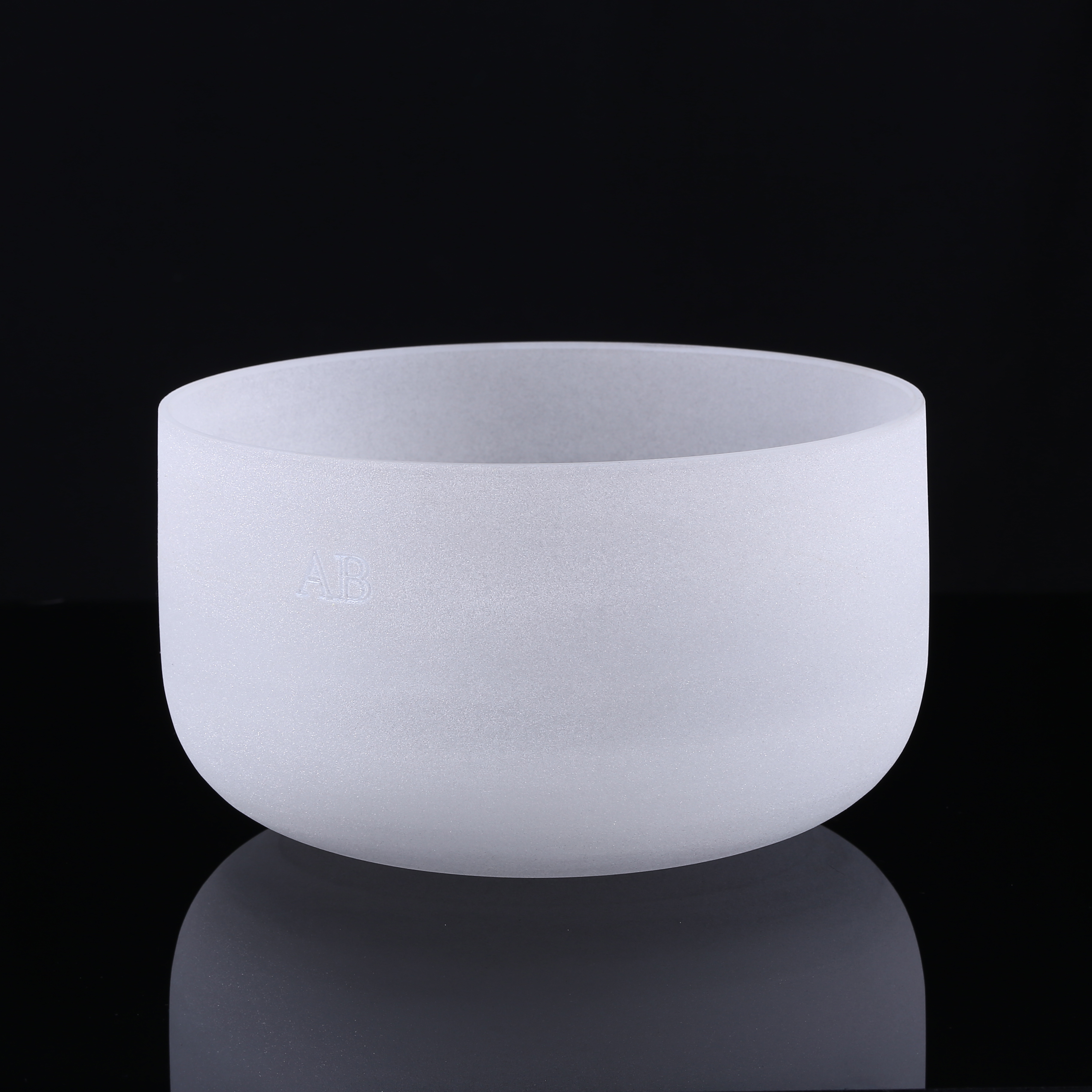
High Temperature Fused Silica Quartz Crucible
View Product Specifications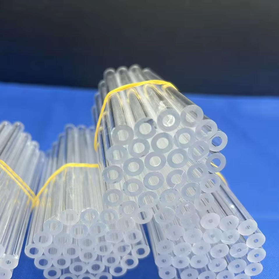
Customized Size Clear Quartz Glass Tube BET Test Tube
View Product Specifications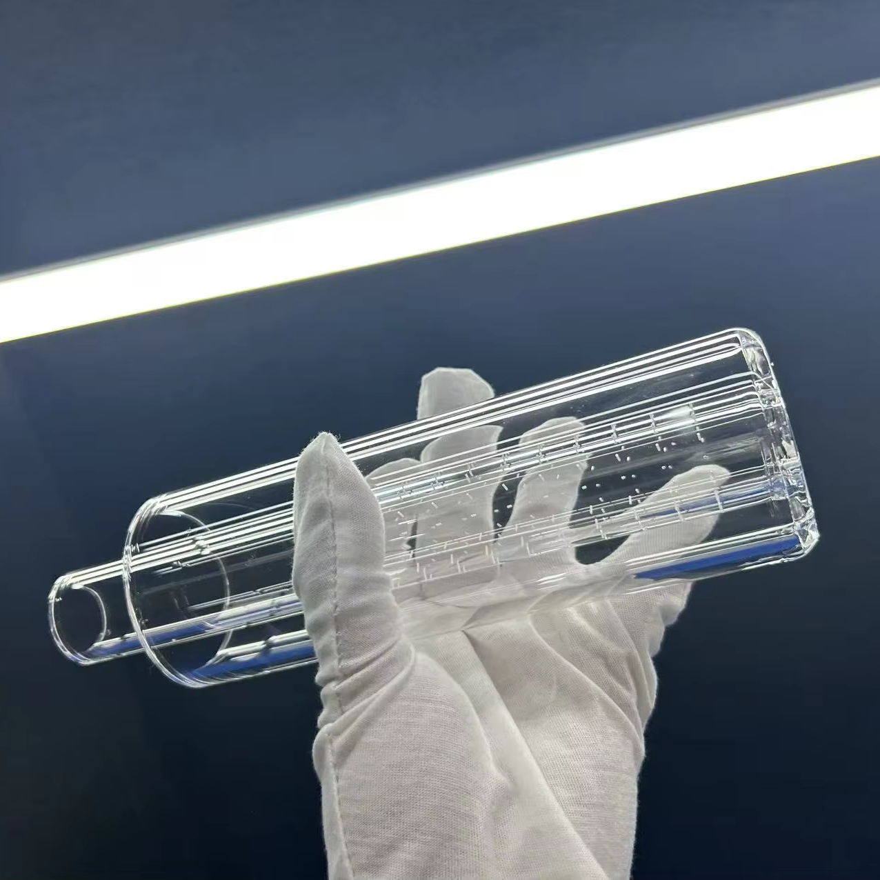
Customized Perforated Quartz Tube for Process Reactors
View Product Specifications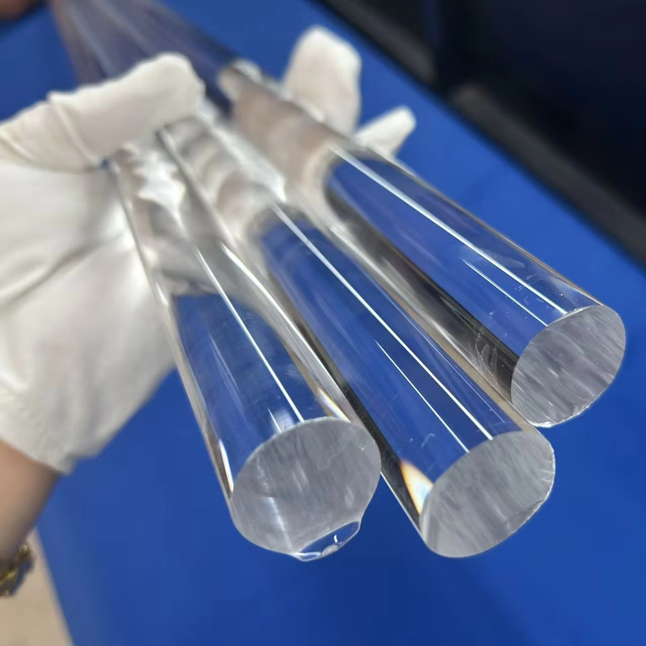
High-Purity Fused Quartz Round Rods & Custom Fabrication
View Product Specifications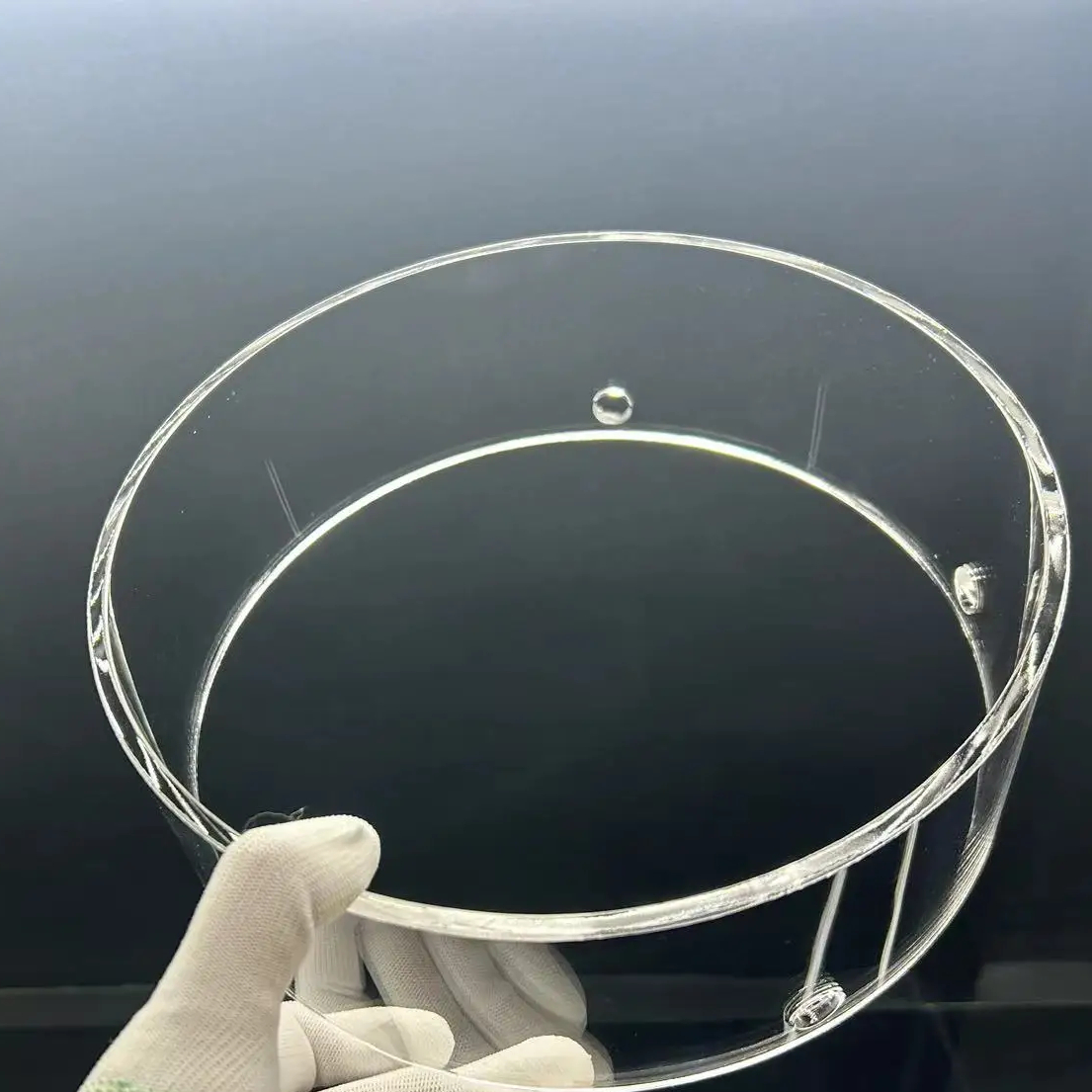
Fused Transparent High Thermal Resistance Quartz Tube
View Product Specifications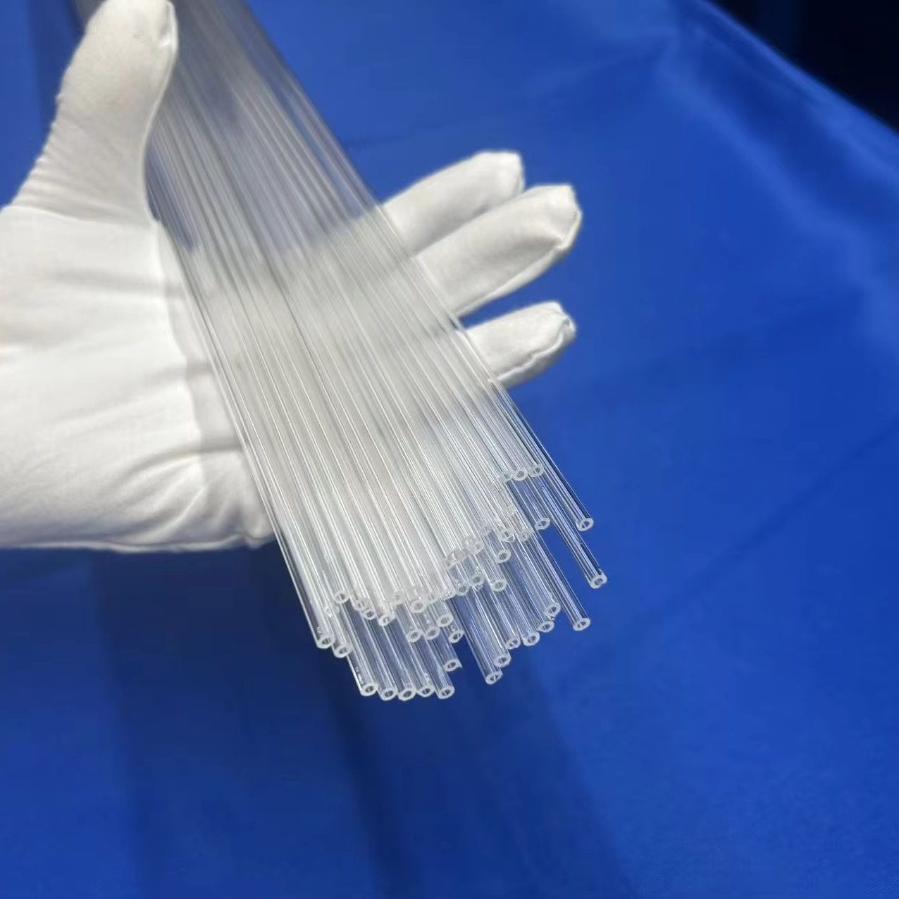
Precision Capillary Quartz Tube for Precision Instruments
View Product Specifications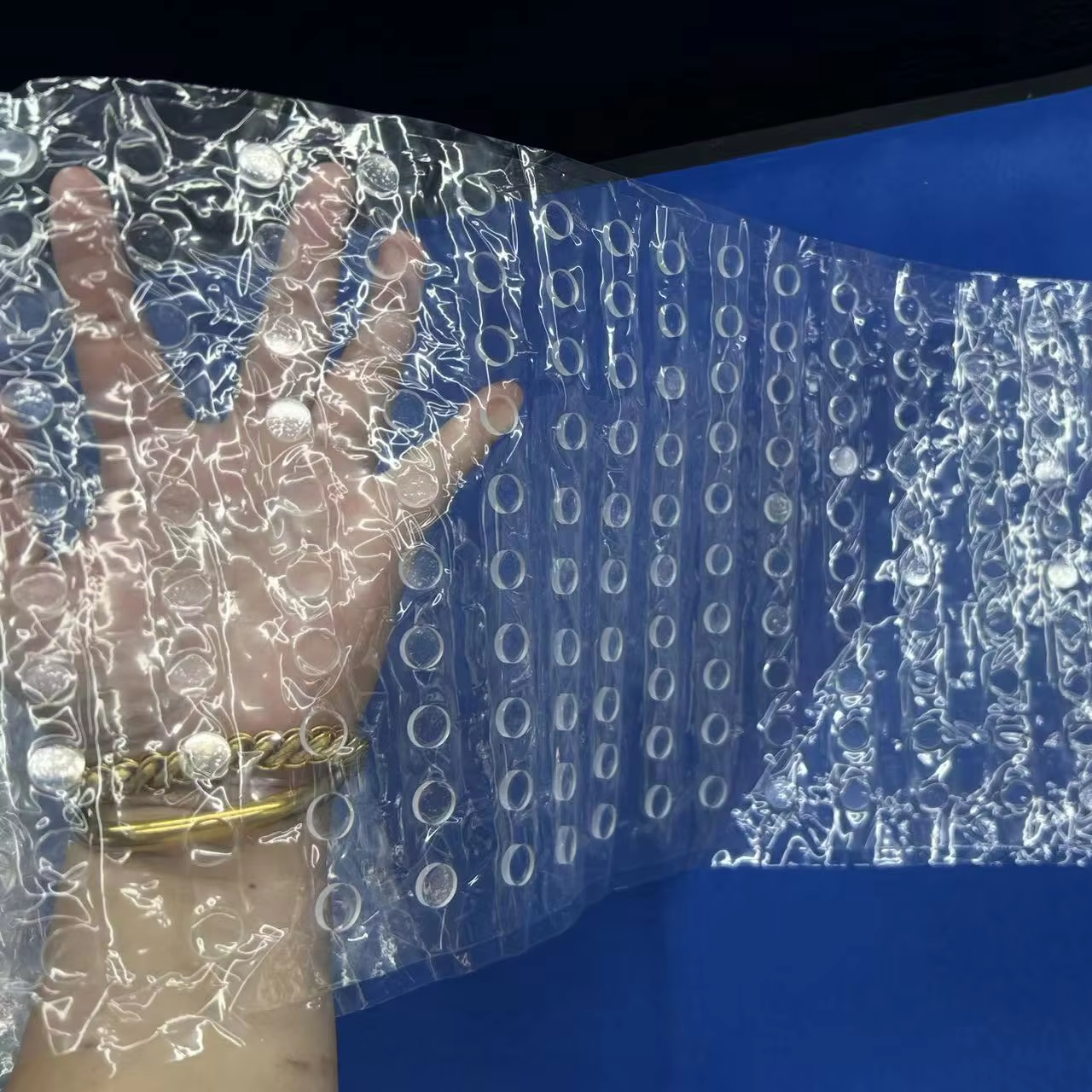
High-Purity Small Size Quartz Wafer with Precision Polishing
View Product Specifications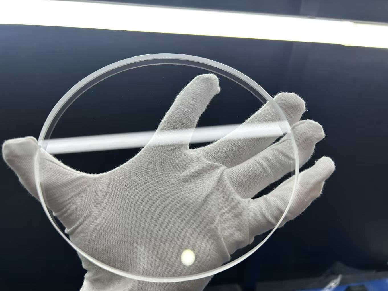
Custom Clear Fused Quartz Glass Sheet for Optics & PV
View Product SpecificationsOptical Sapphire Substrates & Fused Quartz Material Science
Engineering guide to monocrystalline sapphire (Al₂O₃) crystal orientations, synthetic fused silica optical properties, chemical vapor deposition (CVD) compatibility, and structural thermal durability in microelectronics.
In high-stakes semiconductor manufacturing, optoelectronic packaging, and high-energy laser optical trains, optical substrate integrity dictates long-term yield and thermal stability. As a premier CE Certified Optical Sapphire Substrate Supplier & Exporter operating out of Donghai County, Jiangsu (China’s primary crystal and high-purity quartz industrial node), Donghai County Nivra Quartz Products Co., Ltd. delivers precision-engineered sapphire wafers and fused silica optics built strictly to international OEM/ODM tolerance standards.
Single Crystal Sapphire (Al₂O₃) Orientation Guide
Monocrystalline sapphire is anisotropic, meaning its electrical, optical, and mechanical properties vary according to its crystallographic lattice plane. Understanding crystallographic orientation is vital for epitaxy, optical windows, and pressure viewports:
C-Plane Sapphire (0001)
The primary substrate orientation for III-V nitride thin films. C-plane sapphire is widely utilized for GaN (Gallium Nitride) LED growth, blue-violet laser diodes, and high-frequency RF micro-devices due to minimal lattice mismatch with GaN epitaxial layers.
R-Plane Sapphire (1012)
Favored in Silicon-on-Sapphire (SOS) microelectronic circuits and hetero-epitaxial growth. R-plane substrates allow seamless deposition of single-crystal silicon layers, enabling radiation-hardened microprocessors and ultra-fast CMOS RF switches.
A-Plane Sapphire (1120)
Provides uniform dielectric properties and high mechanical strength perpendicular to the C-axis. Ideal for optical windows, high-temperature sight glass windows, and substrates requiring uniform non-birefringent optical paths.
Comprehensive Material Property Comparison: Sapphire vs. Fused Silica Grades
To streamline material procurement for international R&D engineering teams, the following cross-reference table contrasts monocrystalline optical sapphire against our standard high-purity fused quartz grades (JGS1, JGS2, JGS3).
| Material / Grade | Crystallinity | Spectral Bandpass | Thermal Expansion | Refractive Index | Max Temp (°C) | Primary Industrial Applications |
|---|---|---|---|---|---|---|
| Optical Sapphire (Al₂O₃) | Single Crystal | 170 nm – 5.5 µm | $5.0 - 6.6 \times 10^{-6} /^\circ\text{C}$ | 1.768 @ 633 nm | 2000 °C | GaN Epitaxy, Aerospace Sight Windows, Sensor Cover Glass, Micro-LEDs |
| JGS1 Synthetic Silica | Amorphous (SiO₂) | 185 nm – 2500 nm | $5.5 \times 10^{-7} /^\circ\text{C}$ | 1.458 @ 589 nm | 1100 °C | Deep-UV Laser Optics, Photolithography Masks, UV Cuvettes |
| JGS2 Fused Quartz | Amorphous (SiO₂) | 220 nm – 2500 nm | $5.5 \times 10^{-7} /^\circ\text{C}$ | 1.458 @ 589 nm | 1150 °C | High-Temperature Sight Glasses, Flanges, Standard Optical Windows |
| JGS3 IR Grade Quartz | Amorphous (Low OH) | 260 nm – 3500 nm | $5.5 \times 10^{-7} /^\circ\text{C}$ | 1.458 @ 589 nm | 1200 °C | Infrared Pyrometry, High-Thermal Process Tubes, CO₂ Laser Optics |
Future Procurement Trends in Sapphire Substrates & Precision Optics
Strategic foresight into supply chain dynamics, 8-inch/12-inch substrate scaling, Mini/Micro-LED expansion, and environmental compliance requirements shaping buyer procurement through 2030.
1. Large-Diameter Scaling (6" to 8"+ Wafers)
Driven by cost efficiencies in mass LED manufacturing and power electronics, optical substrate procurement is shifting rapidly from standard 2-inch and 4-inch sizes toward 6-inch and 8-inch monocrystalline sapphire wafers. Producing large-diameter sapphire with minimal Total Thickness Variation (TTV < 2 µm) and low internal stress requires advanced Kyropoulos (KY) crystal growth methods and multi-wire diamond sawing.
2. Mini/Micro-LED Display Surge
Next-generation consumer displays, AR/VR headsets, and automotive HUDs rely heavily on Micro-LED technology. Micro-LED fabrication demands double-side chemical-mechanical polished (CMP) C-plane sapphire substrates with near-zero atomic defects and atomic flat surface roughness ($Ra < 0.2\text{ nm}$) to facilitate seamless mass transfer of sub-10 µm LED chips.
3. CE & Sustainability Compliance
Global procurement directors are enforcing strict supply chain audits. Substrate exporters must verify compliance with European CE directives, REACH chemical safety standards, and RoHS environmental directives. Closed-loop diamond slurry recycling and eco-friendly slicing technologies are becoming essential supplier qualification criteria.
Sapphire Processing & Custom Quartz Fabrication Technology
From raw crystal growth in high-temperature furnaces to ultra-precision CNC grinding, laser dicing, and flame annealing in our Donghai facilities.
Precision Laser Scribing & Dicing
Utilizing picosecond and femtosecond UV laser cutting machinery, we produce ultra-clean sapphire wafer edges and custom geometries with negligible Heat-Affected Zones (HAZ) and zero micro-chipping, ensuring structural integrity during high-rpm spinning processes.
Atomic Chemical Mechanical Planarization (CMP)
Our multi-step CMP polishing lines deliver sub-nanometer surface roughness ($Ra < 0.2\text{ nm}$) on both single-sided (SSP) and double-sided (DSP) polished substrates, meeting stringent optical wave-front distortions ($\lambda/10$ @ 632.8 nm).
Thermal Stress Relief & Annealing
High-temperature vacuum annealing furnaces (up to 1800 °C) eliminate lattice dislocation stresses induced during crystal growth and slicing, ensuring that optical sapphire substrates remain perfectly flat under severe operational heating.
Why Direct Buyers Partner with Donghai County Nivra Quartz
Integrated manufacturing from raw material sourcing to final export inspection in Lianyungang, Jiangsu.
Geographic Hub
Headquartered in Donghai County (285 Heping East Road, Lianyungang), China's crystal capital, giving us direct access to world-class raw silica and synthetic sapphire crystal stocks.
101–200 Expert Workforce
Founded in Feb 2019, our skilled workforce operates advanced CNC glass lathes, double-sided optical polishers, flame welding rigs, and laser inspection instruments.
CE & ISO Quality Control
Verified business status, ISO-compliant dimensional tolerance verification (±0.005 mm), and CE certification ensure total reliability for European and American OEMs.
Global Export Expertise
Serving North America (40%), Western Europe (20%), Eastern Europe (14%), and South America (11.4%) with shockproof, fumigation-free wooden export packaging.
Frequently Asked Questions Regarding Sapphire & Quartz Sourcing
Clear engineering and commercial answers to simplify global procurement decision-making.
CE Certified Optical Sapphire Substrates are monocrystalline single-crystal aluminum oxide ($\text{Al}_2\text{O}_3$), offering extreme surface hardness (Mohs 9), exceptionally broad optical transmittance (170 nm to 5.5 µm), and operational thermal resistance above 1700 °C. Unlike standard borosilicate or soda-lime glass, sapphire resists harsh chemical plasma etchants (HF/gas phase) and exhibits high thermal conductivity, making it ideal for semiconductor substrate processing and high-stress optical viewports. CE certification guarantees strict compliance with European safety, dimensional precision, and material purity directives.
When requesting a quote, specify the desired plane: C-plane (0001) for GaN LED/semiconductor growth, R-plane (1012) for Silicon-on-Sapphire (SOS) electronics, or A-plane (1120) for uniform optical windows. Additionally, specify off-cut orientation (e.g., C-plane off-axis by 0.2° to 2.0° toward the M-axis), surface roughness ($Ra$), Total Thickness Variation (TTV), Bow, Warp, and whether Single-Side Polished (SSP) or Double-Side Polished (DSP) finish is required.
Standard stock items ship within 3 to 7 business days. Custom fabrications requiring dedicated wire dicing, CNC machining, or specialized CMP polishing typically take 2 to 3 weeks following drawing approval. Prototype runs and sample orders are welcomed before full-scale OEM mass production.
JGS1 is synthetic fused silica optimized for deep-UV applications (transmitting down to 185 nm) with zero bubble inclusions. JGS2 is a high-grade fused quartz widely used for visible and near-UV optical windows, sight glasses, and process tubes. JGS3 is an infrared-grade fused silica engineered with extremely low hydroxyl content ($\text{OH} < 5\text{ ppm}$), allowing superior IR transmission up to 3500 nm without OH absorption dips.
Fragile quartz tubes, wafers, crucibles, and sapphire substrates undergo ultrasonic cleaning, vacuum sealing in dust-free plastic wrap, and custom embedding into high-density ESD foam shells. Shipments are packed inside reinforced export cartons or fumigation-free wooden crates equipped with drop/tilt indicator labels to guarantee zero breakage during ocean or air transport.
Request Custom Optical Sapphire Substrate & Quartz Quotations
Need precision-polished C-plane/R-plane/A-plane sapphire wafers, JGS1/JGS2/JGS3 optical windows, or custom fused silica labware? Connect with our engineering sales team for rapid quote turnaround within 5 hours.
Send an Inquiry