Engineering Optical Grade Fused Silica: Structural Purity & CE Regulatory Benchmarks
In advanced photonics, excimer photolithography (193 nm / 248 nm), and 3D semiconductor packaging, substrate integrity determines operational fidelity. Amorphous silicon dioxide (SiO₂ ≥ 99.999%) provides anomalous thermal stability, an ultra-low coefficient of thermal expansion (CTE 0.54 × 10⁻⁶/K), and uncompromised optical transmittance from deep ultraviolet (DUV) through mid-infrared (MIR) spectral regimes.
Featured CE-Certified Fused Silica & Quartz Glass Products
Fabricated to DIN ISO 10110 standards with CNC ultrasonic profiling, chemical-mechanical planarization (CMP), and certified flame fire-polishing.
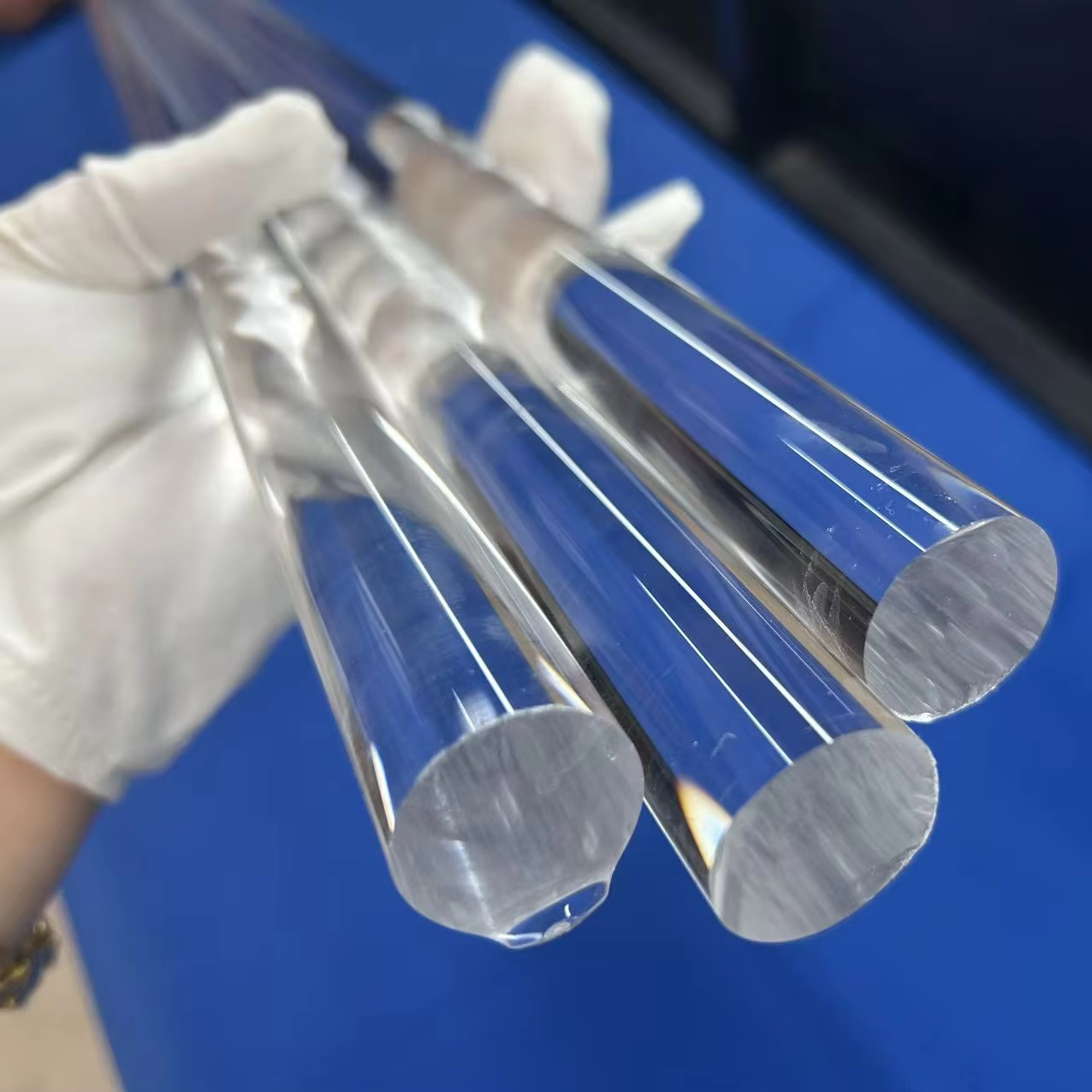
High-Purity Fused Quartz Large Diameter Round Rods
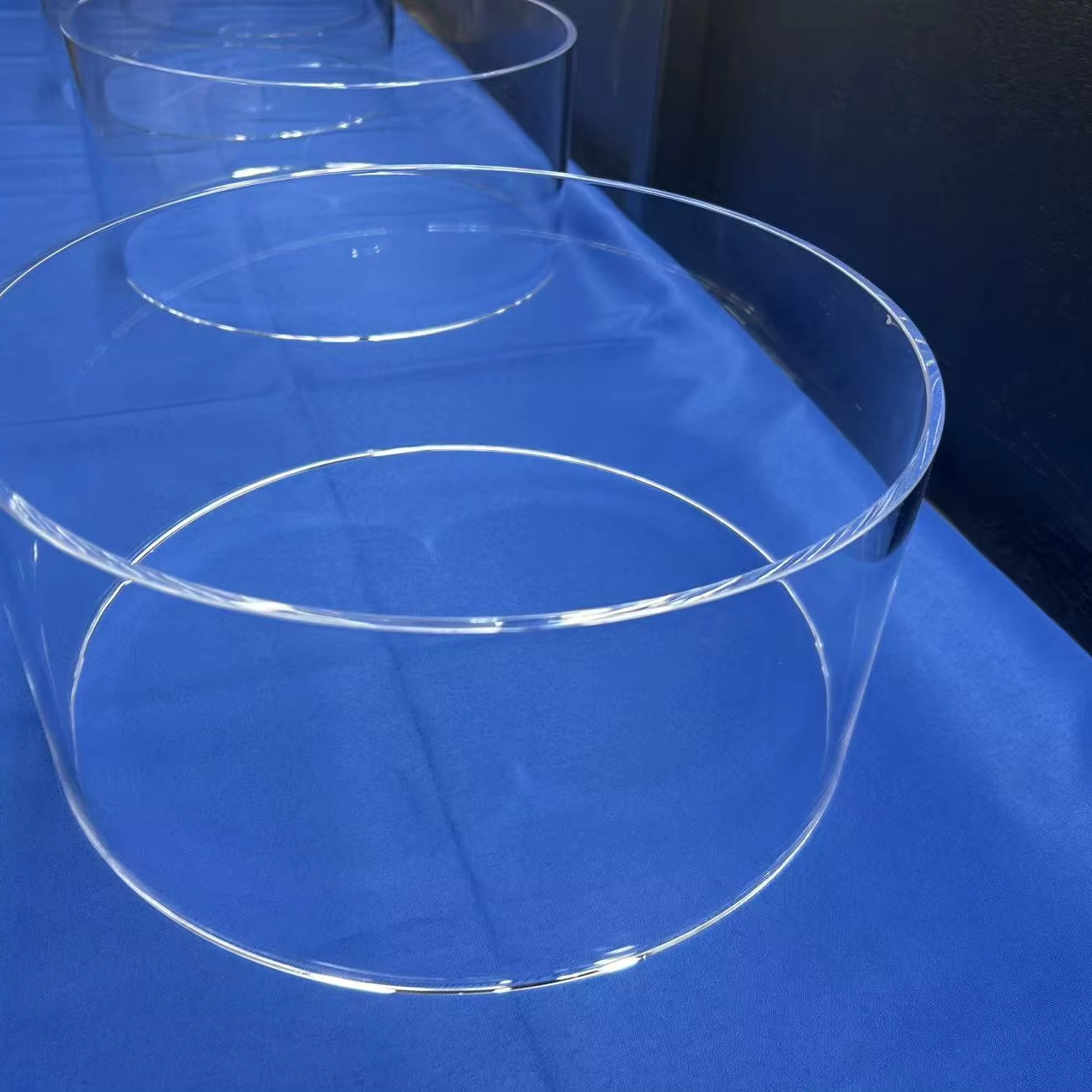
Industrial Fused Quartz Large Diameter Round Rods
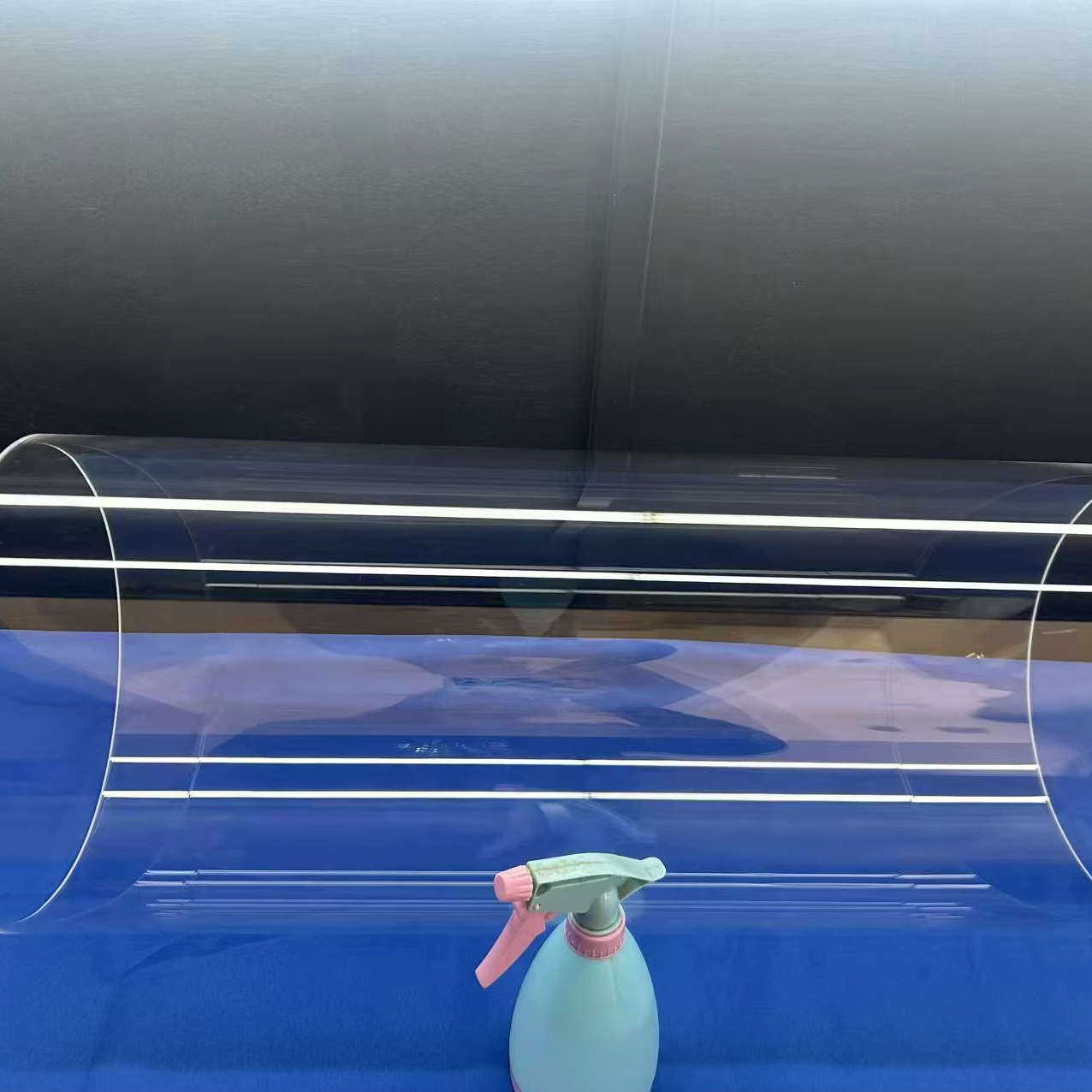
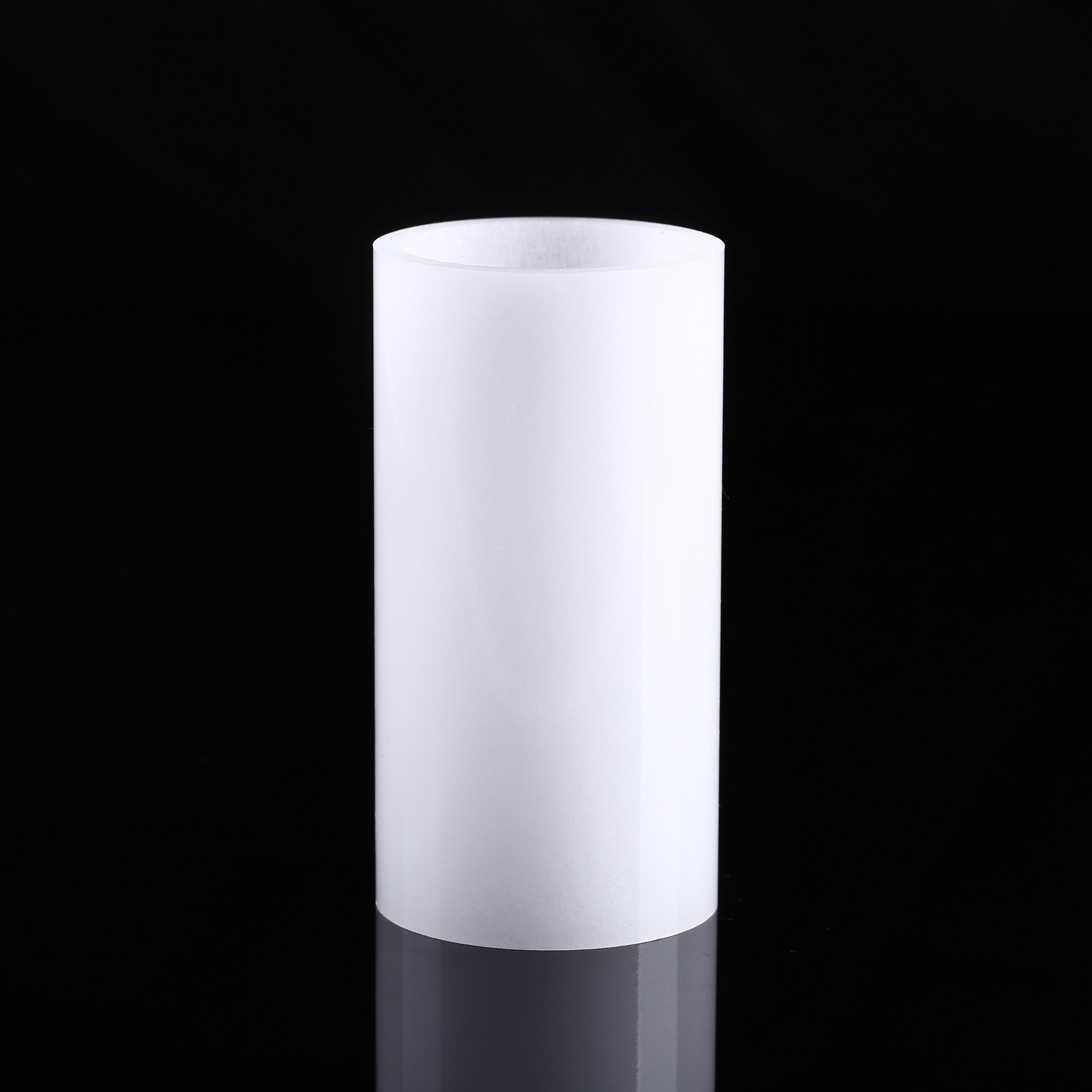
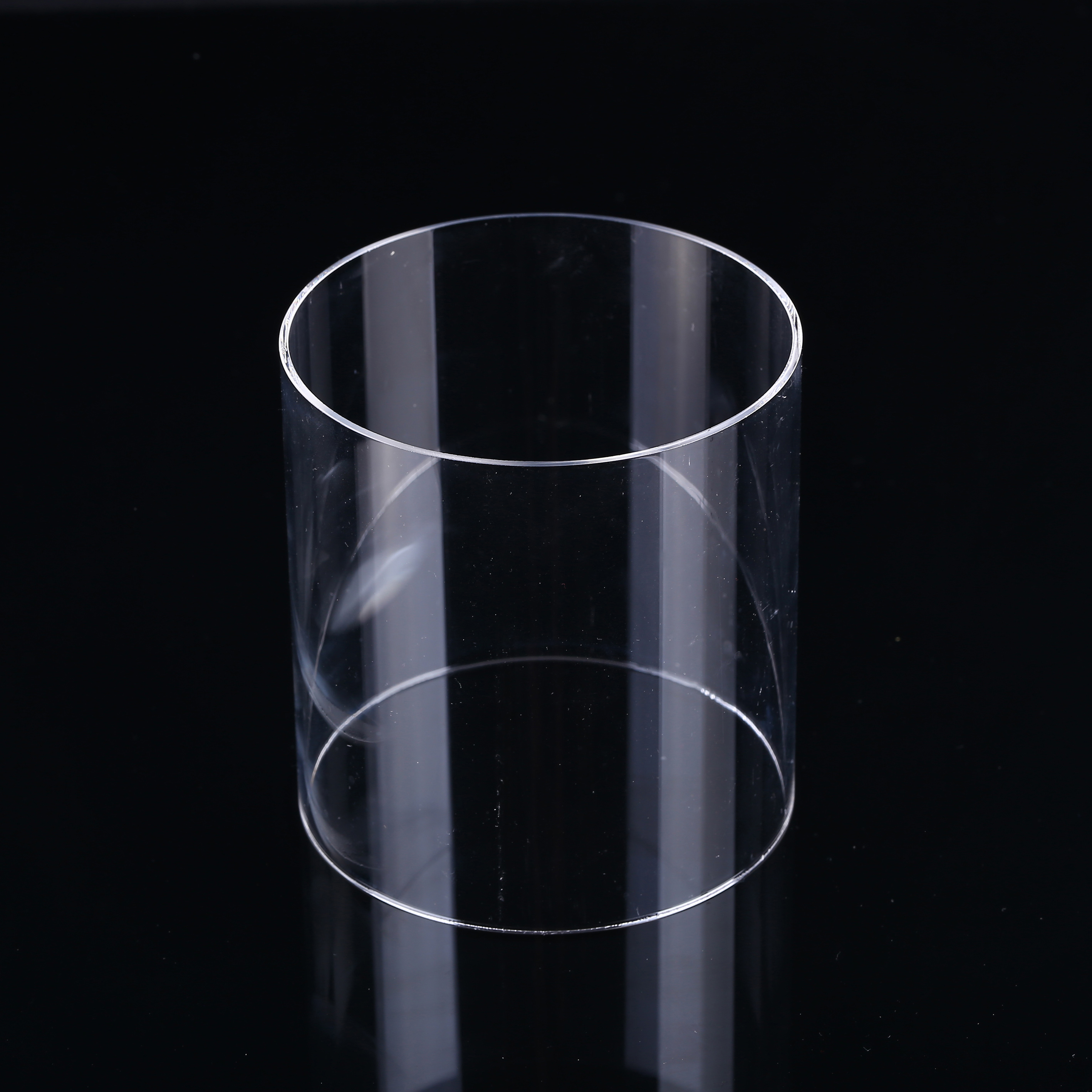
Customizable High Purity Fused Quartz Glass Tube
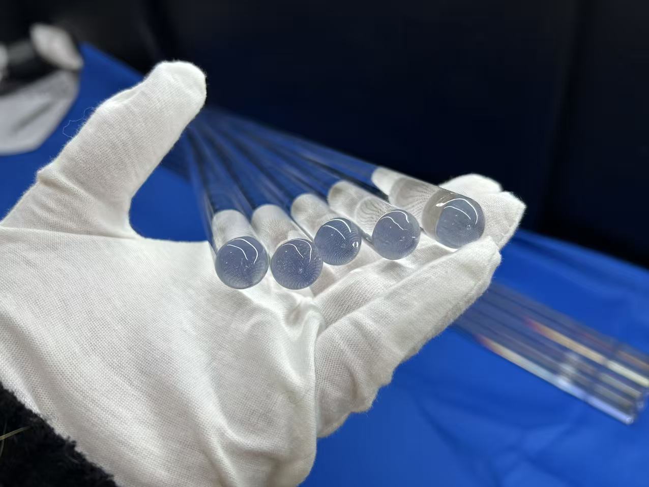
Precision Finished Fused Quartz Round Rod Stock
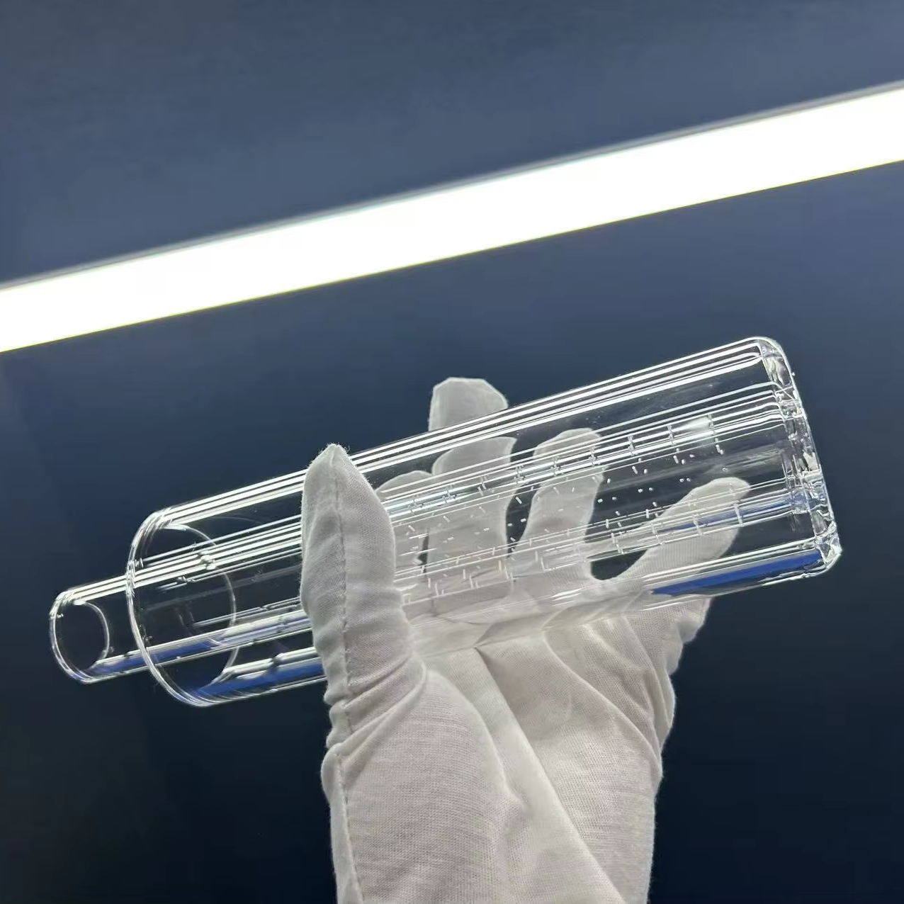
Customized Perforated Quartz Diffusion Tube
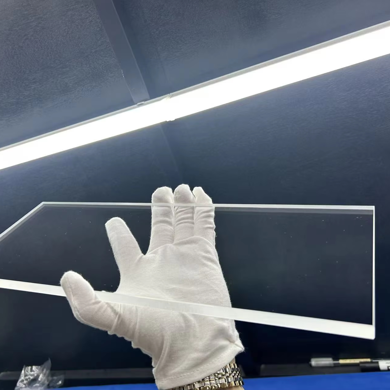
Ultra Clear High Purity Quartz Substrate Sheet
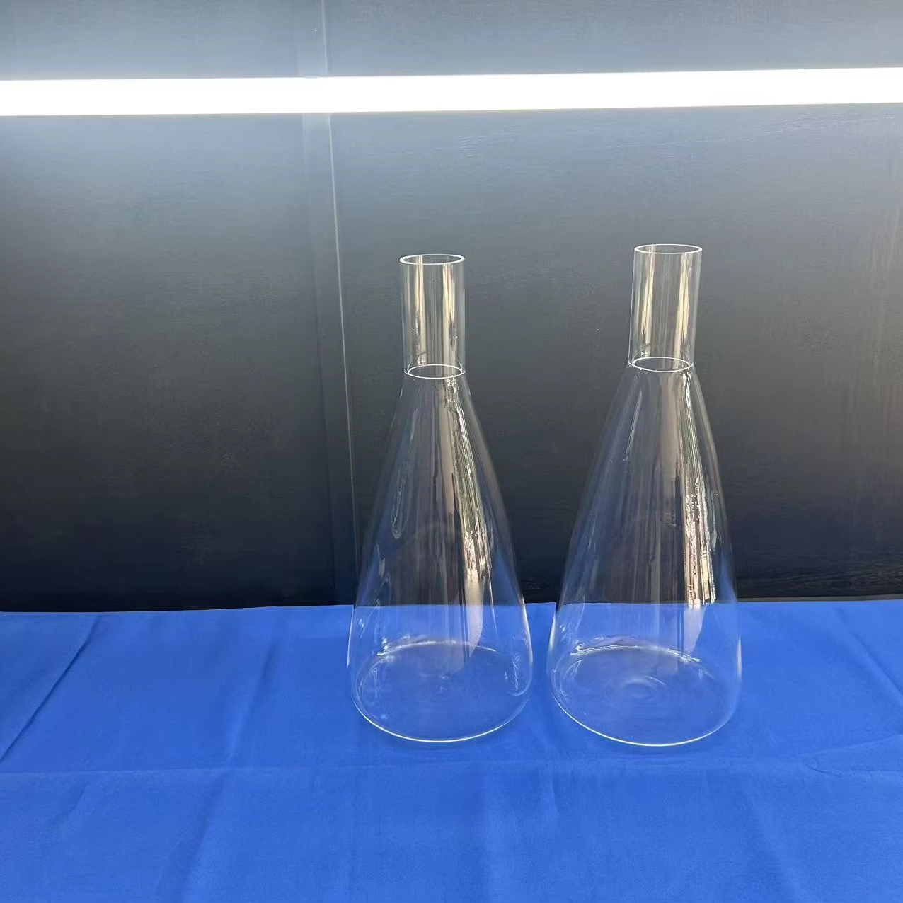
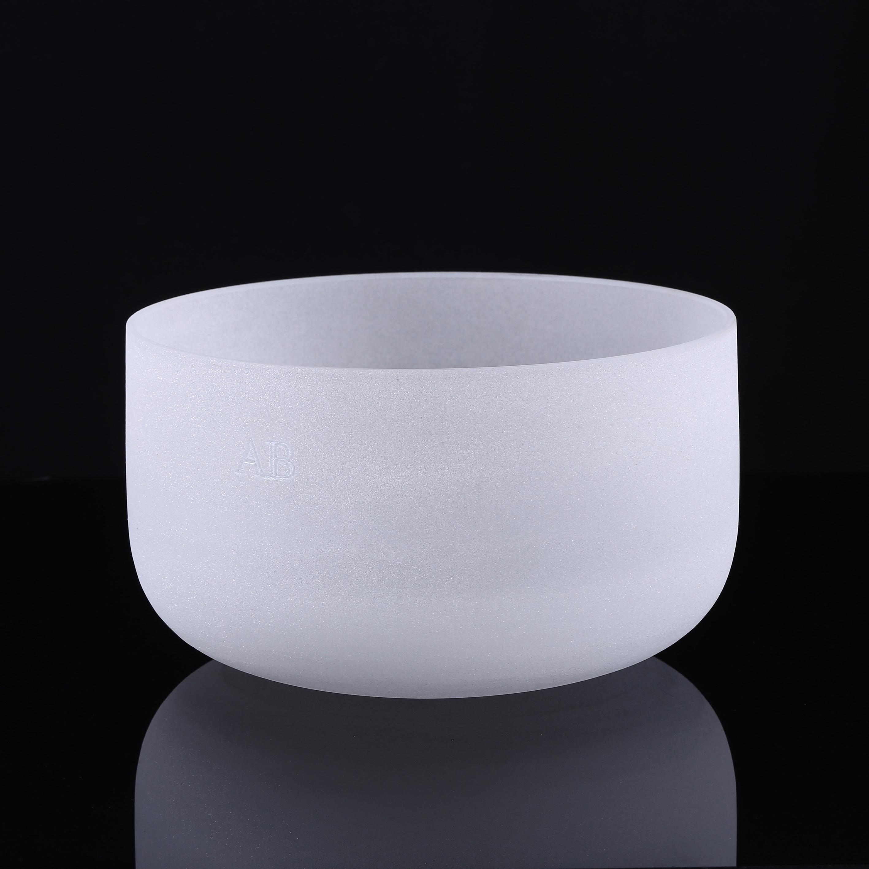
Laboratory Fused Silica Quartz Glass Reaction Flask
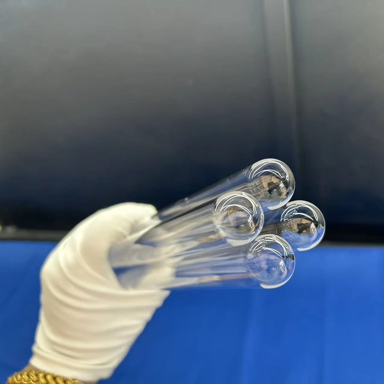
Fused Silica Bottom Sealing Tubes (20-25mm)
Synthetic Silica (JGS1) vs. Fused Natural Quartz (JGS2/JGS3) Performance Matrix
Selecting the exact silica substrate grade requires balancing transmission bands, hydroxyl ion concentration, refractive index homogeneity, and bubble class standards under ISO 10110-3.
| Substrate Grade | Transmission Band (T ≥ 85%) | Hydroxyl (OH⁻) Content | Refractive Homogeneity (Δn) | Laser Damage Threshold (LIDT) | Primary Industrial Application |
|---|---|---|---|---|---|
| JGS1 (Synthetic Silica) | 185 nm – 2,500 nm (DUV to NIR) | < 5 to 1,200 ppm (Grade dep.) | 1 × 10⁻⁶ (Class A / 4 directions) | > 25 J/cm² @ 1064nm, 20ns, 20Hz | Excimer Photolithography, DUV Laser Mirrors, UV Cuvettes |
| JGS2 (Optical Fused Quartz) | 220 nm – 2,500 nm (UV to NIR) | 30 – 150 ppm | 4 × 10⁻⁶ (Standard Grade) | > 12 J/cm² @ 1064nm, 20ns, 20Hz | Laser Protective Windows, High-Pressure Viewports, UV Lamps |
| JGS3 (Infrared Fused Quartz) | 260 nm – 3,500 nm (Water-free IR) | < 5 ppm (Zero 2.73 µm absorption) | 2 × 10⁻⁵ (Thermal Optical) | > 15 J/cm² @ 1064nm, 20ns, 20Hz | FTIR Spectroscopy, Mid-IR Sensor Windows, Pyrometry Optics |
| Semiconductor Fused Quartz | Visible – Broadband Near-IR | < 30 ppm | Non-Interferometric Grade | Not Laser Rated | Diffusion Furnaces, Quartz Boats, CMP Carriers, Epitaxy Tubes |
Extreme Thermal Shock Resistance
Features a linear expansion coefficient of 5.4 × 10⁻⁷ /°C between 20°C and 320°C. Plates survive quenching from 1100°C directly into ice water without micro-fracturing or planar distortion.
Dielectric & RF Transparency
Dielectric constant ε = 3.75 @ 1 MHz, dissipation factor tan δ < 0.0001. Ideal as low-loss dielectric carriers in semiconductor RF plasma chambers and high-frequency microwave windows.
Acid & Plasma Inertness
Resistant to all commercial acids including aqua regia and fuming nitric acid at boiling temperatures, experiencing dissolution only when exposed to Hydrofluoric (HF) acid and concentrated phosphoric acid above 300°C.
Why Top Sourcing Teams Partner With Nivra Quartz
From raw mineral synthesis to certified European compliance, we eliminate multi-tier supply chain markups while implementing full trace-element traceability.
Cluster Advantage at Donghai
Headquartered at 285 Heping East Road, Lianyungang, we tap directly into China’s primary silica supply chain. This geographic consolidation enables factory-direct raw billet access, rapid furnace turnaround, and significant cost savings passed directly to OEM clients worldwide.
CE & International Compliance
Every component batch complies with the European Low Voltage Directive principles where applicable, RoHS 3 (Directive 2015/863/EU), and REACH regulations. We verify zero hazardous plasticizers or prohibited heavy metal impurities, verified via ICP-OES spectral chemical assays.
Full-Spectrum Precision Machining
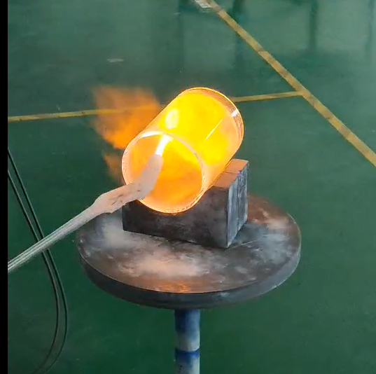
Equipped with ultrasonic milling centres, double-sided planetary lapping benches, continuous hydrogen-oxygen glassblowing lathes, and high-temperature vacuum annealing lehrs. We produce intricate drilled flanges, laser-perforated manifolds, and laser polished optical surfaces under one roof.
Strategic Procurement Dynamics in the High-Purity Fused Silica Ecosystem
Procurement executives face a transforming landscape governed by sub-2nm microelectronics, glass-core packaging transitions, and supply security directives.
Glass Core Substrate Migration
As organic interposers hit thermal and mechanical thresholds in AI high-bandwidth computing, leading foundries are shifting to fused silica glass-core panels. Sourcing strategies are actively locking down high-volume supplies of low-warp, ultra-flat (TTV < 1 µm) 510×515 mm silica panels.
Dual-Source Supply De-Risking
Geopolitical export limitations and raw silicon tetrachloride volatility have catalyzed dual-sourcing architectures. Tier-1 photonics and medical OEMs are prioritizing validated manufacturing partners who maintain local raw crystal stocks and independent melting capacity in established production clusters.
Extreme Damage Threshold Optics
Demand for multi-kilowatt fiber lasers and ultra-fast picosecond/femtosecond industrial systems has escalated the demand for virtually defect-free substrates. Purchasing criteria now emphasize low subsurface damage (SSD < 50 nm) and minimal bubble-inclusion distributions (Class 0 per ISO 10110-3).
ESG & Carbon Footprint Scrutiny
European buyers now mandate detailed energy declarations for electric arc-fusion versus flame-hydrolysis operations. Procurement protocols favor facilities implementing closed-loop slurry recovery systems and oxy-hydrogen regenerative burners to lower the embodied Scope 3 carbon intensity of delivered silica parts.
Technological Horizons: Nanoscale Finishing & Micro-Machining
Advancements in surface topology control and micro-additive silica forming are unlocking performance parameters once considered unattainable.
Super-Polishing (Ra < 0.1 nm)
Magnetorheological Finishing (MRF) and ion beam figuring (IBF) are becoming industrial standards for high-energy laser substrates. These non-contact polishing regimes eradicate sub-surface micro-fractures, mitigating laser-induced thermal lensing and pushing transmission figures to theoretical Fresnel limits across high-power laser optical trains.
FLICE 3D Microfluidics
Femtosecond Laser-Induced Chemical Etching (FLICE) enables arbitrary 3D monolithic channel routing within solid fused silica blocks. This breakthrough allows high-precision lab-on-a-chip bio-reactors, capillary electrophoresis chips, and optical waveguide arrays with zero adhesive bonding seams or thermal delamination risks.
High-Selectivity Plasma Etching
Next-generation reactive ion etching (RIE) protocols using optimized fluorocarbon chemistries achieve vertical Through-Glass-Vias (TGV) with aspect ratios exceeding 20:1. This enables ultra-dense electrical interconnects across fused silica interposers, crucial for next-tier quantum computing processors and optoelectronic co-packaging.
Frequently Asked Technical Questions on Fused Silica Procurement
Direct answers addressing technical tolerances, packaging protocols, and certification verifications for procurement engineers and quality auditors.
What differentiates JGS1, JGS2, and JGS3 from a functional sourcing perspective?
JGS1 is synthetic fused silica synthesized from silicon compounds via vapor-phase axial deposition (VAD) or flame hydrolysis. It boasts no particulate inclusions, zero bubbles (Class 0), and unmatched deep-UV transmission down to 185 nm, making it essential for UV lasers, photolithography, and UV analytical instruments.
JGS2 is fabricated from naturally occurring high-purity quartz crystal via electric arc fusion. It transmits efficiently across 220 nm to 2500 nm. It represents the most economical optical-grade choice for standard viewport windows, UV lamp envelopes, and furnace view ports.
JGS3 is manufactured using an electric vacuum fusion process to extract water content, lowering OH⁻ concentration to under 5 ppm. This eradicates the pronounced 2.73 µm water absorption band, making it the choice for infrared spectroscopy, thermal imaging optics, and mid-IR laser optics.
What does CE Certification mean for fused silica substrates and quartz glass?
While unworked glass raw material is an inert substance, quartz fabricated into laboratory equipment, pressure sight windows, optical flow cells, or electrical lamp envelopes must comply with European safety norms. For quartz laboratory assemblies, CE marking confirms conformity with EN 61010-1 (Safety requirements for electrical equipment for measurement, control, and laboratory use). When integrated into pressurized containment, it adheres to essential safety parameters of the Pressure Equipment Directive (PED 2014/68/EU). Furthermore, full regulatory conformance entails compliance with RoHS Directive 2011/65/EU (and 2015/863 amendment) and REACH (EC 1907/2006), verifying absence of restricted substances such as lead, mercury, hexavalent chromium, and SVHCs.
What standard surface quality and flatness tolerances are achievable on custom substrates?
Standard production tolerances deliver surface roughness Ra ≤ 0.5 nm, scratch-dig standards of 20-10 or 10-5 per MIL-PRF-13830B, and surface flatness (transmitted wavefront distortion) of λ/10 to λ/20 @ 632.8 nm across the clear aperture. Total Thickness Variation (TTV) can be held under 1 µm with parallelism better than 3 arcseconds. For ultra-precision wafer geometries (such as 100mm, 150mm, 200mm, and 300mm SEMI standard wafers), double-sided planetary CMP ensures pristine, stress-free subsurface conditions.
How does Nivra Quartz ensure zero breakage and scratch prevention during international export?
Fragile quartz parts require rigorous multi-barrier packaging. Optical substrates, wafers, and polished discs are ultrasonically cleaned and packed within Class 100 anti-static cleanroom wafer cassettes or membrane vacuum boxes that prevent physical contact with polished surfaces. Bulk tubes and heavy rods are individually sleeved in dense cross-linked polyethylene (EPE) closed-cell foam, suspended within reinforced structural cartons, and placed in ISPM-15 compliant fumigation-free solid timber plywood crates with built-in shock/drop indicators.
What is the typical prototype lead-time and Minimum Order Quantity (MOQ)?
Standard quartz components (tubes, rods, standard optical blanks) carry low entry thresholds with MOQ starting at 1 to 10 pieces to facilitate engineering evaluation. Small precision wafers, laser windows, and discs typically start at 25 to 50 pieces. Prototype turnarounds from CAD/STEP drawings generally take 7 to 10 business days, inclusive of dimensional CMM reports and spectrophotometer transmission scans.
How do you verify internal strain and residual birefringence in finished quartz parts?
Residual stress created during thermal cutting or flame lathe fabrication causes optical distortion and vulnerability to spontaneous catastrophic fracture under thermal shock. Every finished component undergoes fine annealing in programmable electric lehrs with slow cooldown cycles below the strain point (1075°C). Strain birefringence is certified using dual-polarization polariscopes, guaranteeing optical path difference (OPD) ≤ 5 nm/cm for interferometric and laser-grade optics.
Accelerate Your Precision Quartz Procurement Today
Upload your technical drawings (.DXF, .DWG, .STEP, or .PDF) along with target purity, transmission criteria, and dimensional tolerances. Our senior optical engineers in Donghai provide manufacturability feedback and factory-direct quotation within 5 hours.