Choosing a supplier for a High Purity Quartz Wafer takes more than comparing quoted prices. Purity levels, wafer dimensions, surface finish, and batch consistency can all affect performance. Even small variations may matter in demanding laboratory, optical, or semiconductor-related processes. Details count.
This guide introduces ten suppliers worldwide and compares the information buyers need to assess their fit. It considers stated material grades, available wafer formats, manufacturing capabilities, quality documentation, and technical support. Where public specifications are limited, that gap deserves attention rather than assumption. A polished product page is not the same as independently verified performance.
Supplier capabilities can change, and “high purity” does not always mean the same thing across product lines. Buyers should confirm the applicable specification, measurement method, tolerances, and certificate documentation directly with each company. Ask about sample availability, lead times, packaging, and how defects or out-of-spec batches are handled. Those practical questions reveal a lot.
The list is intended as a comparison starting point, not a universal ranking or endorsement. A supplier suited to custom research orders may not fit repeat production needs. Likewise, the lowest price may bring trade-offs in consistency or support. This overview aims to make those differences easier to spot, while leaving room for careful verification.
What High-Purity Quartz Wafers Are and Where They Are Used
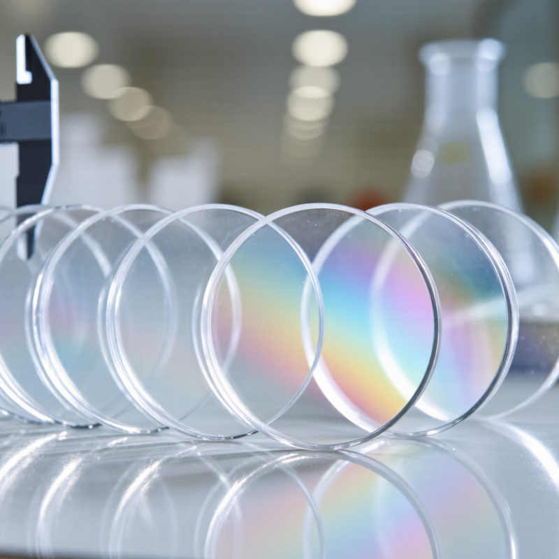
High-purity quartz wafers are thin, flat discs made from silica-rich quartz, typically fused into a glass-like material. They are not the same as silicon wafers. Their value comes from low levels of metallic contamination, chemical stability, and good transmission of ultraviolet and visible light. Exact purity requirements vary by process, so “high purity” alone does not guarantee suitability.
That distinction matters. In semiconductor research and manufacturing, quartz wafers can serve as transparent substrates, process carriers, or components in equipment exposed to heat and reactive chemicals. They also appear in optical systems, laboratory devices, and some microfluidic applications, where viewing a fine channel or sample is useful. SEMI reported that global semiconductor materials sales reached US$67.5 billion in 2024, including US$42.1 billion in wafer-fabrication materials. This figure covers many materials, not quartz alone, but it reflects the scale of the manufacturing ecosystem these wafers serve. A practical selection check is the wafer’s trace-metal specification, thickness tolerance, surface finish, and thermal history. Small defects matter. Terminology can be confusing, and specifications should be matched to the actual process rather than judged by a purity label alone.
Top 10 High Purity Quartz Wafer Suppliers Worldwide – What High-Purity Quartz Wafers Are and Where They Are Used
Supplier-neutral sourcing guide covering ten common product and capability segments. The entries are not company listings or a ranked supplier list. “Quartz wafer” may refer to crystalline quartz or to amorphous fused silica; these materials have different properties and applications.
| Product or Supplier Capability Segment | Typical Material and Form | Common Applications | Key Sourcing Considerations |
|---|---|---|---|
| Single-crystal piezoelectric quartz wafers | Crystalline quartz cut to a specified orientation; commonly supplied as polished wafers or blanks. | Frequency-control resonators, oscillators, and piezoelectric components. | Specify crystal cut and orientation, thickness, surface finish, flatness, and allowable defects. |
| AT-cut quartz wafer capability | Rotated-cut crystalline quartz designed for temperature-stable resonator applications. | Quartz crystal resonators and frequency-control devices. | Confirm cut angle tolerance, wafer thickness, electrode compatibility, and the required frequency range. |
| ST-cut quartz wafer capability | Crystalline quartz cut used in piezoelectric device designs requiring specific frequency and temperature behavior. | Resonators, sensors, and other piezoelectric devices. | Check cut orientation, dimensional tolerances, surface quality, and device-specific performance requirements. |
| Quartz substrates for surface acoustic wave devices | Oriented crystalline quartz wafers selected for their piezoelectric and acoustic properties. | Surface acoustic wave filters, delay lines, and sensing devices. | Match crystal orientation and propagation direction to the device design; review surface finish and contamination limits. |
| Quartz substrates for MEMS and sensors | Crystalline quartz wafers, often supplied with custom dimensions or patterned features. | MEMS structures, inertial sensors, pressure sensors, and piezoelectric sensors. | Confirm wafer diameter, thickness, orientation, bonding compatibility, and whether patterned or bare wafers are required. |
| High-purity fused silica wafers | Amorphous silica glass, commonly described as fused silica; it is not a piezoelectric single crystal. | Optical substrates, microfluidic devices, and selected semiconductor or laboratory applications. | Specify optical transmission range, surface quality, thickness uniformity, and relevant impurity limits. |
| UV-grade fused silica substrates | High-transmission fused silica selected for ultraviolet optical use. | UV optics, photonics, and optical components used in ultraviolet systems. | Request transmission data at the operating wavelengths and verify surface finish, homogeneity, and coating requirements. |
| Optical-grade crystalline quartz wafers | Crystalline quartz polished for optical use; its optical behavior differs from amorphous fused silica. | Optical components and applications that make use of quartz’s birefringent properties. | Specify crystal orientation, optical-axis alignment, transmission range, and whether polarization behavior is important. |
| Custom-diameter and custom-thickness wafer fabrication | Crystalline quartz or fused silica cut and polished to customer-defined dimensions. | Research prototypes, custom sensors, optical assemblies, and specialized production runs. | Confirm achievable dimensions, edge treatment, thickness tolerance, flatness, lead time, and minimum order quantity. |
| High-purity wafer finishing and inspection | Quartz or fused silica wafers supplied with controlled polishing, cleaning, and inspection. | Applications sensitive to particles, scratches, surface contamination, or optical defects. | Define inspection methods, particle and defect criteria, packaging cleanliness, and whether purity data refer to bulk material or surface contamination. |
Material note: High-purity silica products are often specified by SiO₂ content, but the stated purity alone does not describe every trace impurity or surface contaminant. Compare material type, cut, dimensions, finish, and application-specific test data before selecting a supplier.
FAQS
Check trace impurities, wafer dimensions, flatness, surface roughness, and edge quality. A clean surface alone proves little.
Request certificates, thickness maps, roughness measurements, inspection records, and batch traceability. Confirm test methods and acceptance limits.
Ask how trace impurities are measured and whether calibrated methods are used. Similar numbers may come from different tests.
Cutting, lapping, polishing, cleaning, and packaging can affect wafer quality. Ask which steps are controlled in-house.
No. A sample shows potential, not batch-to-batch consistency. Still, one sample can fool us.
Send each candidate the same drawing and inspection criteria. Compare actual records, not stated tolerances alone.
Test samples under your actual process conditions. Look for thickness variation, surface damage, and particles. Details matter.
Silicon wafer shipment data describes that market, not quartz-wafer demand. High-purity quartz supply information is limited.
Packaging should protect surfaces from particles during transit. Check the wafers after delivery, too. That step is easy to miss.
Conclusion
This article explains what a High Purity Quartz Wafer is and why its carefully controlled material quality makes it useful in precision manufacturing, research, and other demanding technical applications. It outlines how buyers can compare suppliers worldwide by considering product consistency, technical expertise, production capacity, documentation, and quality controls, rather than relying on a single measure or broad claims.
The guide also reviews the capabilities and standards that may distinguish ten supplier profiles, including wafer dimensions, purity levels, surface finish, customization options, and inspection processes. It shows how to match these specifications with an application’s performance requirements, order volume, and delivery expectations. By clarifying the questions to ask and the details to verify, the article helps buyers assess potential suppliers and make a more informed choice.